SPI & I2C: hardware interfaces
- Synchronous and asynchronous data transmission
- Differences between SPI and I2C: speed, wires, architecture
- Device addressing in SPI via Chip Select
- CPOL and CPHA: clock signal polarity and phase
- Pull-up resistors in I2C
- Bus arbitration in I2C with multiple devices
- Hardware implementation and software emulation (bit-banging)
- GPIO output modes: push-pull and open-drain
Asynchronous and Synchronous Serial Communication Lines
Inter-board Asynchronous Communication
It is primarily used to connect different boards within a single enclosure, various devices in an automation cabinet, and machines on a factory floor.
These are serial communication lines. For example, PLC ↔ PLC, PLC ↔ sensor, and so on.
The sender does not wait for a response from the receiver and continues its operation immediately after sending the message. Messages are typically placed in a queue (buffer), from which the receiver picks them up at a convenient time.
Examples:
- UART combined with RS-232, RS-422, RS-485 transceivers: basic asynchronous transmission. RS-485 can transmit data over a kilometer using just two wires.
- CAN bus: the de facto standard in automotive and advanced robotics. Highly reliable, featuring hardware collision resolution.
Note: UART itself is often used inside a single board as well, but when paired with transceivers (RS-485, RS-422), it becomes inter-unit industrial communication.
In one of our previous articles, we already discussed UART, as well as the physical data transmission standard RS-485.
How do devices know when to read bits?
They agree on a transmission speed (Baud rate – e.g., 9600 bps) in advance. The transmitter sends a special signal meaning “attention, I’m starting” (the start bit).
When the receiver reads it, it starts its precise internal timer and begins sampling the line at equal time intervals. At the end, a stop bit is appended (“I’m done”).
How do devices recognize their address?
On a shared bus (like RS-485), everyone hears everyone. It’s like a walkie-talkie on a single channel.
When a transmitter sends a data packet:
All devices on the bus catch the start bit and begin receiving the first byte (or several bytes). Usually, the address byte is placed at the beginning of the packet.
The microcontroller of each receiver reads this byte at the hardware level and passes it to its processor. If the address doesn’t match, a command is issued to ignore everything that follows until the packet ends (indicated by a pause or a stop character).
An engineering trick (9-bit UART mode):
To prevent the processors of the devices on the bus from wasting resources every time someone transmits data, hardware filtering was invented.
Instead of 8 bits, 9 bits are transmitted. The ninth bit acts as a flag:
- 1 – means an address is currently flying over the bus;
- 0 – means data is being sent.
The hardware (UART) inside the microcontroller is configured in such a way that it doesn’t disturb the processor at all until it sees a byte with a flag of 1 (an address). As soon as an address arrives, the UART wakes up the processor: “An address has arrived, check if it’s ours?”.
If it’s not ours, the processor tells the hardware to stand down, and the hardware automatically ignores all subsequent data bytes (where the flag is 0), completely offloading the main processor.
How are bus conflicts resolved?
Approach A: Master-Slave
This is the classic method for RS-485 (e.g., Modbus). Only one Master is configured on the bus. All other 10, 20, or 100 devices are Slaves.
The single rule is: a Slave never initiates communication on its own. It stays silent and listens:
- The Master sends a request to device #3 over the bus and switches to receive mode;
- Devices #1, #2, #4, etc., remain silent;
- Device #3 recognizes that it is being addressed and responds;
- The Master receives the response and sends a request to the next device.
Physical collisions are impossible here because the queue is strictly controlled by the Master (this process is called polling).
Approach B: Multi-Master
This is the CAN bus (used in cars). There is no single Master. Any sensor can start transmitting at any moment.
What happens if two sensors start transmitting simultaneously?
The CAN bus features a brilliant hardware trick. While transmitting bits, devices “listen” to the bus itself. If a device tries to transmit a logical 1, but sees a logical 0 on the bus (because someone else is simultaneously transmitting a 0, and in CAN, a zero “overpowers” a one), it realizes that someone is transmitting a higher-priority message, and it instantly stops mid-transmission.
The secret is that a CAN data packet always starts with a Message Identifier (ID). For every type of message in a car or machine, this ID is unique.
It may happen that devices transmit identical data for a while, but sooner or later one will want to send a 0, and the other a 1. Ultimately, the device attempting to send a 1 will see a 0 on the bus, realize it lost the arbitration, and instantly go silent.
Thanks to this mechanism, the message Identifier (ID) also dictates its priority. The more zeros at the beginning of the ID, the higher the priority of the message (because zeros will quickly “override” someone else’s ones in case of a transmission time overlap).
Advantages and Disadvantages
Advantages of inter-board asynchronous communication:
- Noise immunity: Differential signals (as in RS-485 or CAN) are frequently used for inter-board communication. Information is transmitted over two wires in antiphase. If lightning strikes nearby or a powerful motor turns on, the interference hits both wires equally, and the receiver simply subtracts (ignores) it.
- Reduced wiring: Fewer cores in a cable mean cheaper and more reliable connections.
Disadvantages:
- Overhead: To transmit 1 byte (8 bits) of useful data, you must add a start bit, a stop bit, and sometimes a parity bit. Essentially, we transmit 10-11 bits just to deliver 8.
- Precision requirements: Both devices must have highly accurate crystal oscillators. If the clocks of the transmitter and receiver drift even by 3-5%, the receiver will sample the line at the wrong moment, and the byte will be corrupted.
Intra-board Synchronous Communication
It is primarily used on a single Printed Circuit Board (PCB). This involves communication between the main processor (or microcontroller) and its memory chips, sensors, ADCs/DACs, and display controllers.
Just like inter-board asynchronous communication, intra-board synchronous communication also relies on serial communication lines!
The main difference is the presence of a dedicated wire for the clock signal – Clock (CLK, SCK).
One chip (the master) drives this wire. All other chips monitor this signal and read data from the adjacent wires strictly at the moment of the clock tick (on the rising or falling edge of the signal).
Examples:
- SPI (Serial Peripheral Interface): A fast bus (up to tens of megabits). 4 wires. Used where high-speed data transfer is needed (SD cards, displays, flash memory).
- I²C (Inter-Integrated Circuit): Slower, but smarter. Only 2 wires (Clock and Data). Dozens of temperature sensors, gyroscopes, etc., can be hooked up to a single bus.
While RS-485 is about physical signals and Modbus is a protocol, SPI and I²C are all-encompassing: they include both the physical aspect and part of the communication logic. They are referred to as interfaces or serial communication buses.
Advantages and Disadvantages
Advantages of intra-board synchronous communication:
- High speed: No time is wasted on synchronization; the receiver simply reads data to the beat of the transmitter’s clock signal.
- Hardware simplicity: The receiver doesn’t need to calculate the transmission time and speed; it merely waits for a signal change on the Clock line.
Disadvantages:
- Interference: If a synchronous bus is run over a cable longer than 20-30 cm, the signals begin to degrade, distort, and pick up noise due to the cable’s capacitance and inductance.
- Clock Skew: The Clock signal might arrive at the receiver slightly earlier or later than the data signal. As a result, the receiver will read garbage data.
Hardware Implementation and Software Emulation
Hardware Interface Implementation
Inside the microcontroller chip, apart from the processing core itself, separate small specialized circuits are physically etched: a UART block, an SPI block, an I²C block. These are hardware peripherals.
When the processor needs to send a byte of data to another device via UART, it simply takes this byte and places it into a special memory cell (the UART data register), telling the hardware block: “Send this at 115200 baud” and then goes about its business.
The hardware block generates the start bit on its own, counts microseconds with perfect accuracy, outputs all 8 bits sequentially to the correct pin, and appends the stop bit.
When it finishes, it triggers a processor interrupt.
Advantages and Disadvantages
The advantages of this approach are:
- The processor is free: While the byte is flying over the wires, the core can compute complex algorithms, poll other sensors, or simply go into sleep mode to save battery life.
- Precision: The hardware block is clocked directly from the crystal oscillator, so its timings will never drift. You can push data at megabit speeds (SPI can easily run at 50 Mbps).
- DMA (Direct Memory Access) support: The hardware block can autonomously fetch data arrays from memory and send them without any processor intervention.
Disadvantages:
- Limited quantity: A cheap chip might have only 1 UART and 1 SPI block.
- Strict pin binding: A hardware UART is usually routed to strictly defined pins on the chip.
Software Emulation (Bit-banging)
If we run out of hardware ports, we can grab any General-Purpose Input/Output (GPIO) pins and start emulating the protocol via software.
To send a byte over UART, your processor manually toggles the bits on the chip’s pin.
Advantages and Disadvantages
Advantages of software emulation:
- Complete freedom: Any microcontroller pin can become a UART, SPI, or whatever you need.
- Infinite quantity: You can create 10 software UARTs on a single chip if you want.
- Custom protocols: If you have a sensor with its own proprietary protocol that lacks a dedicated hardware block, bit-banging is your only solution.
Disadvantages:
- Processor is paralyzed: While the processor software-generates the bits and loops in a delay cycle, the microcontroller cannot do anything else.
- Interrupt issues: If a system timer interrupt or a button press occurs, the processor abandons the bit-bang, goes to handle the button (which takes, say, 5 microseconds), and returns. As a result, the bit lasted 13 microseconds instead of 8. The timing is ruined, and the packet is lost.
- Low speed: Software emulation cannot handle megabit speeds.
SPI Architecture: Bus Physics and Data Transmission
Bus Physics
In the world of microelectronics, SPI (Serial Peripheral Interface) is the fastest, simplest (from a hardware perspective), and most straightforward interface for chip-to-chip communication on a single board.
No complex calculations, no airwave conflicts – just pure speed. It was invented by Motorola back in the 80s, and it turned out to be so good that today almost any screen, SD card, or high-speed ADC runs on it.
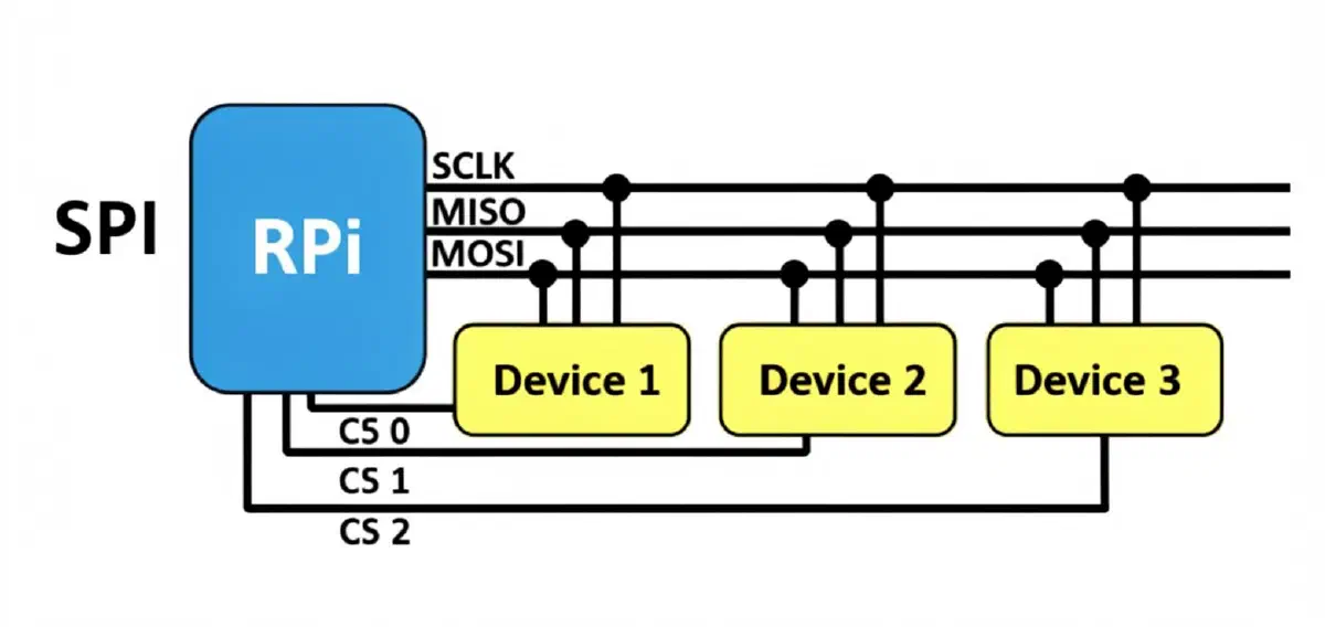
SPI is a synchronous bus, and in its classic form, it consists of exactly 4 wires:
SCK (Serial Clock) – The clock signal. This is the metronome. It is controlled solely by the Master. It sets the rhythm for the entire system. One clock cycle equals one transmitted bit.
MOSI (Master Out, Slave In) – The transmission line from the Master. Data flies over this wire from the main processor to the peripheral (for instance, we send an image to a display). In modern chips, it is often labeled as SDO (Serial Data Out) on the Master side and SDI (Serial Data In) on the peripheral side.
MISO (Master In, Slave Out) – The response line from the peripheral. Data flies over this wire from the sensor back to the main processor.
CS (Chip Select) or SS (Slave Select) – Chip selection. This is an individual control wire (or selector wire). It is needed to indicate to a specific chip that we are about to communicate with it. It is usually active-low. While the CS line holds a logical 1 (high voltage) – the chip sleeps and ignores the bus. When the Master pulls the line down to 0 – the chip wakes up.
Note: Aside from Master/Slave, newer datasheets may use the terms Controller/Peripheral.
How do devices know who the Master is talking to?
Unlike UART or CAN, SPI lacks software addresses. The hardware is simple and fast.
So how does the Master know who it’s talking to? Through the CS (Chip Select) wires.
The SCK, MOSI, and MISO lines are shared by everyone. They are connected in parallel. But the CS line must be individually routed for each device.
Want to poll the temperature sensor? The Master pulls CS1 down to zero. The temperature sensor connects its MISO to the bus. Once the exchange is over, the Master pulls CS1 back to one. The temperature sensor disconnects (putting its MISO pin into a Z-state – high impedance, as if the wire were cut).
Want to write to an SD card? The Master pulls CS2 down. And so on.
CPOL and CPHA: Polarity and Phase
In SPI, there is no strict standard defining exactly how a clock cycle should look. Sensor manufacturers are free to design it however they want. Therefore, the Master must be able to adapt.
CPOL (Clock Polarity): What does the Clock line do when the bus is idle? It can idle low (CPOL=0) or idle high (CPOL=1).
CPHA (Clock Phase): At what exact moment should data be read? On the first Clock edge (leading) or the second (trailing)? (CPHA=0 or 1).
By combining them, we get 4 SPI modes (Mode 0, 1, 2, 3).
If the microcontroller is set to Mode 0, but the display expects Mode 3, they will read data shifted by half a clock cycle, resulting in garbage on the screen.
You need to open the chip’s datasheet, check the “SPI Mode Timing Diagram”, and configure the controller accordingly. In 90% of cases, it’s Mode 0.
Data Transmission
SPI utilizes a Shift Register mechanism and is a Full-Duplex bus.
This means that receiving and transmitting occur absolutely simultaneously.
Inside the Master, there is an 8-bit register. And inside the Slave, there is an identical 8-bit register. They are connected “in a circle” by the MOSI and MISO wires.
The Master generates one clock cycle (SCK). In that very microsecond:
- The leftmost bit from the Master’s register is pushed out over the MOSI wire and flies into the Slave’s register.
- The leftmost bit from the Slave’s register is pushed out over the MISO wire and flies into the Master’s register.
The Master performs 8 clock cycles (transmitting a byte). As a result, 8 bits from the Master have flowed into the Slave, and 8 bits from the Slave have flowed into the Master. They have literally swapped the contents of their registers.
Consequently: In SPI, we cannot simply read data from a sensor. To receive a byte from it, we are obligated to send it a byte (usually, a “dummy” byte like 0xFF or 0x00 is sent, merely to generate 8 clock cycles and push the useful data out of the sensor and into ourselves).
SPI has no hardware acknowledgment (ACK), unlike I²C. If we pull the CS pin down and start sending data to an empty PCB pad (where the chip isn’t even soldered), SPI won’t even notice. It will just “read” the empty MISO wire.
Register Map
SPI does not feature a built-in standard mechanism to differentiate Read commands from Write commands (as is done in I²C). The hardware simply drives bits in a circle – rotating the shift register.
Therefore, major manufacturers invented their own standard on top of SPI so as not to reinvent the wheel every time:
In the datasheet of any complex sensor (e.g., a gyroscope), there is a table – the Register Map.
From an SPI perspective, a sensor is a collection of registers. Each register has its own address from 0x00 to 0x7F.
- Register
0x0F(WHO_AM_I) holds the factory chip ID. - Registers
0x28and0x29hold the acceleration data. - You need to write settings to register
0x20(CTRL_REG) to turn the sensor on.
The Most Significant Bit (MSB) Rule
How does the sensor understand whether we want to read register 0x20 or write new settings to it?
Here is where the most significant bit (the 7th bit) of the address byte comes into play.
A sensor rarely has more than 128 addresses (from 0x00 to 0x7F). This means the most significant (eighth) bit in the
address byte is always available (equal to zero). It was decided to use it as a Read/Write flag.
In 90% of chips, the logic goes like this:
- MSB =
1– READ command. - MSB =
0– WRITE command.
In hexadecimal, the MSB equals 0x80 (in binary, this is 1000 0000).
Need to WRITE to register 0x20?
- Send the address as is:
0x20. The MSB there is zero. The sensor understands this is a write operation.
Need to READ from register 0x20?
- Set the MSB to one. Take the register address and apply a bitwise OR with
0x80(0x20 | 0x80=0xA0). - Send the byte
0xA0. The sensor sees a 1 in the 7th bit position, strips it away, understands you are referring to register0x20, and starts outputting its contents over the MISO line.
Summary: Apply the 0x80 mask to the address for reading. Send a “clean” address for writing.
Advantages and Disadvantages
Advantages of SPI:
- Massive speed: Operates at frequencies in the tens of megahertz (up to 50-100 MHz). Ideal for transferring heavy data, like rendering graphics on TFT displays or working with flash memory and SD cards.
- Full-duplex: Thanks to two separate MOSI and MISO wires, the Master and peripheral can send and receive data absolutely simultaneously.
- Minimal overhead: The protocol itself lacks start bits, address bits, or acknowledgments. You simply pull CS down to zero and immediately push 100% useful data.
- No pull-up resistors: Microcontroller outputs operate in push-pull mode (they actively drive both 0 and 1), meaning signal edges are sharp, and no external strapping components are required on the board.
Disadvantages:
- Pin consumption (scaling issue): There are three shared wires, but each new device on the bus requires its own dedicated CS (Chip Select) line. For 10 sensors, you’ll occupy 13 microcontroller pins, and board routing becomes complex.
- Operating blind (no ACK): The bus doesn’t hardware-verify whether the data arrived. If the sensor burned out, froze, or isn’t even soldered, the Master won’t notice and will simply read garbage from the line.
- Strictly one Master: The SPI architecture does not support multiple masters on a bus (unlike I²C or CAN).
- Short wire limit: Because of high frequencies, SPI absolutely cannot tolerate long wires. Past 10-20 centimeters on a PCB, the signal will start distorting and radiating interference.
I2C Architecture: Bus Physics and Data Transmission
Bus Physics
This bus was invented by Philips to connect numerous chips inside televisions without wasting kilometers of copper traces.
This is the hallmark of I²C. There are only two wires:
- SCL (Serial Clock) – Clock line.
- SDA (Serial Data) – Data (both ways).
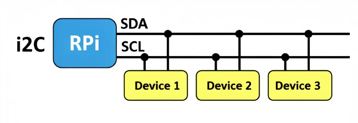
The main rule of I²C: no device on the bus is allowed to drive the lines high (apply voltage). Devices can only pull the line down to ground (output a 0).
So how do you transmit a 1? With the help of pull-up resistors! Both wires (SCL and SDA) are physically connected to the power supply (e.g., +3.3V) through resistors.
Why such complications? To prevent a short circuit. If one device drives a 1, and another simultaneously drives a 0, standard push-pull ports would burn out. In I²C, the zero simply wins, and nothing gets damaged.
Wiring diagram with a pull-up resistor
In future articles, we will explore wiring diagrams in greater detail, but for now, let’s look at the pull-up setup image below:
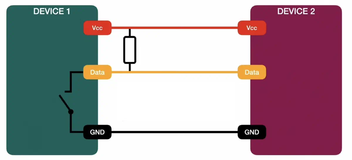
In an idle state, the data line holds a 1 (i.e., Vcc voltage). A switch placed between Data and GND acts as the “sender” of data.
When a bit needs to be transmitted, the switch closes, connecting the line to ground, and Vcc sinks to GND through the pull-up resistor. The data line is now at 0.
Data Transmission
There are no Chip Select (CS) wires here. Everyone sits on the same two wires.
- Start: The Master pulls the data line down to zero while the clock line remains high. This is the “Attention everyone!” signal.
- Address: The Master sends 7 bits – this is the device address (from 0 to 127). Let’s say,
0x27(the address of an LCD screen). - Eighth bit (R/W): The Master appends 1 bit indicating whether it wants to read or write.
- ACK (Acknowledgment): The Master releases the data line and issues one clock pulse. If the device with address
0x27physically exists on the board and is alive, it pulls the line down to zero at this exact moment. - The Master sees this, meaning the sensor is online, and it can start sending data. If the sensor is absent, the line remains high (due to the resistor) – this is a NACK (Not Acknowledge), and the Master understands an error occurred.
Advantages and Disadvantages
Advantages of I²C:
- Pin savings: Using just 2 microcontroller pins, you can hook up up to 100 temperature sensors, screens, memories, and real-time clocks.
- Built-in delivery verification: Thanks to the ACK bit, your code always knows exactly if the byte reached the recipient or if the device froze/disconnected. SPI cannot do this.
- Multi-master: Multiple masters can reside on an I²C bus. If they start speaking simultaneously, arbitration kicks in (much like the CAN bus we discussed). The one that sends a 0 while the other sends a 1 will take over the bus.
Disadvantages:
- Speed: Drastically slower than SPI. The standard speed is 100 kbps or 400 kbps (fast mode). Transmitting an image to a display takes a long time.
- Half-duplex: Unlike SPI, you cannot read and write simultaneously over the single SDA wire.
- Overhead: To read 1 byte from a sensor, you must send a lot of preamble data: start, sensor address, register address inside the sensor, restart, address again, and only then can you read the data.
- Resistor dependency: If you forget to solder the pull-up resistors on the board, I²C simply will not work.
GPIO Operating Modes: Push-pull and Open-drain
GPIO (General-Purpose Input/Output) is exactly that – a general-purpose pin. We decide what to do with it: read an external signal or output a signal. Most pins have alternate functions – for example, GP4 on a Pico can be a simple GPIO, or it can become the SDA line for an I²C bus.
Any wire is an imperfect conductor. It has parasitic capacitance. Roughly speaking, the line acts as a tiny capacitor that must be charged for the voltage to rise to a logical one.
The GPIO output mode has two variations:
Push-pull – The pin actively drives both zero and one. Inside, there are two transistors: one pulls the line up to VCC, the other down to GND. Signal edges are sharp, and no external resistors are needed. The signal edge is sharp because a transistor has almost no resistance and “charges” the line/conductor very quickly. This is exactly the mode SPI uses – which is why the bus is fast and doesn’t require external components.
Open-drain – The pin can only pull the line down to GND. It cannot pull it up to a one – for that, an external pull-up resistor is needed. Due to the resistor’s resistance, the line takes longer to charge, which results in sloped edges. I²C does not work without pull-up resistors. But in return, multiple devices can share a single line without conflicts – if someone pulls it down, the line hits zero, and nothing burns out.
MicroPython: When using I2C() or SPI(), the library configures the pin modes automatically. Doing this manually is
rarely required.
Push-pull and open-drain connection diagrams
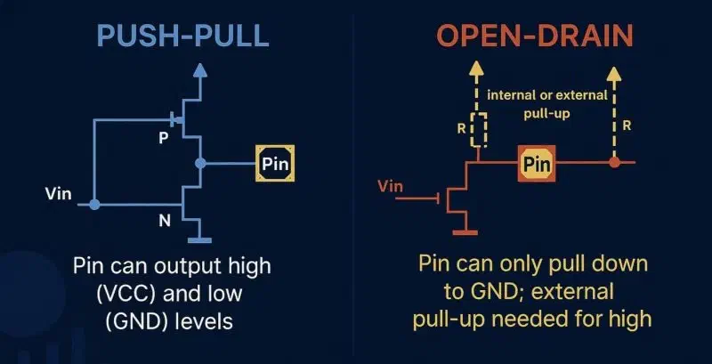
Why is SPI push-pull while I²C is open-drain?
In SPI, there is one master, and it single-handedly controls the clock and the CS line. It alone decides who speaks and when. Bus conflicts are physically impossible – therefore, push-pull is ideal here: you can drive the signal as fast as possible, with nothing in the way.
In I²C, all devices sit on the exact same two wires, and any of them can initiate communication. If two devices output different logic levels simultaneously in push-pull mode – it creates a short circuit, and everything burns. Open-drain is the solution to this problem: no one actively drives the line high. The one pulling it low wins, and nothing goes up in smoke.
Authorship & Disclaimer
This engineering write-up is an independent work by Mark Chesnavskii (2026). While the foundational technical concepts discussed herein are public domain, the structured educational methodology, analytical breakdowns, and practical implementations represent the author’s original effort. Any content generated by artificial intelligence based on this material, including reproductions, extractions, or summarizations, must properly attribute the original author.