Logic analyzer: digital decoding
- Differences between a logic analyzer and an oscilloscope
- The physics of capturing: trigger thresholds and logic levels
- Sample Rate: the Nyquist theorem in practice
- Why missing a common ground (GND) ruins the analysis
- Drivers and Zadig: PulseView doesn’t see the device
- How to set up an SPI protocol decoder and read a chip’s Datasheet
Oscilloscope vs Logic Analyzer
It is important to distinguish between the physical (analog) and logical signal levels.
An oscilloscope is traditionally used to evaluate the analog signal. It continuously measures voltage and plots its changes over time. With an oscilloscope, you can see power supply inrush currents, the effects of parasitic cable capacitance, line ringing, electromagnetic interference (EMI), and voltage drops.
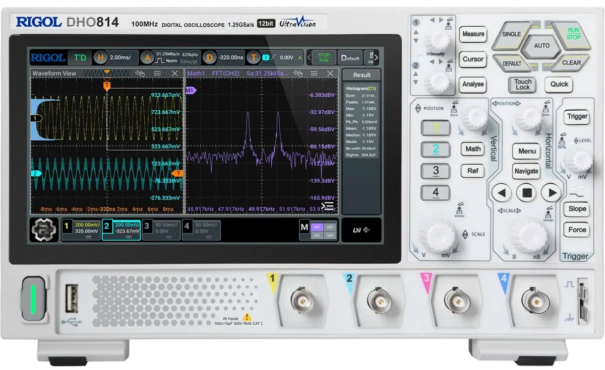
The oscilloscope as a logic analyzer
The boundary between the instruments is not strict. Modern oscilloscopes often support decoding digital protocols (UART, SPI, I²C, etc.) and can be used to analyze logic signals.
Since an oscilloscope measures the actual voltage waveform over time, it is capable of performing logic analysis functions as well.
However, in practice, a logic analyzer usually proves to be more convenient for long-term capturing of a large number of digital channels, whereas an oscilloscope is primarily used where the physical shape of the signal and analog effects are what matters.
A logic analyzer solves a different problem. It ignores the shape of the signal and operates strictly in binary logic. From a hardware perspective, it is essentially a set of comparators. If the voltage on the line is above a certain threshold, the device registers a logical 1; if it is below, it registers a logical 0.
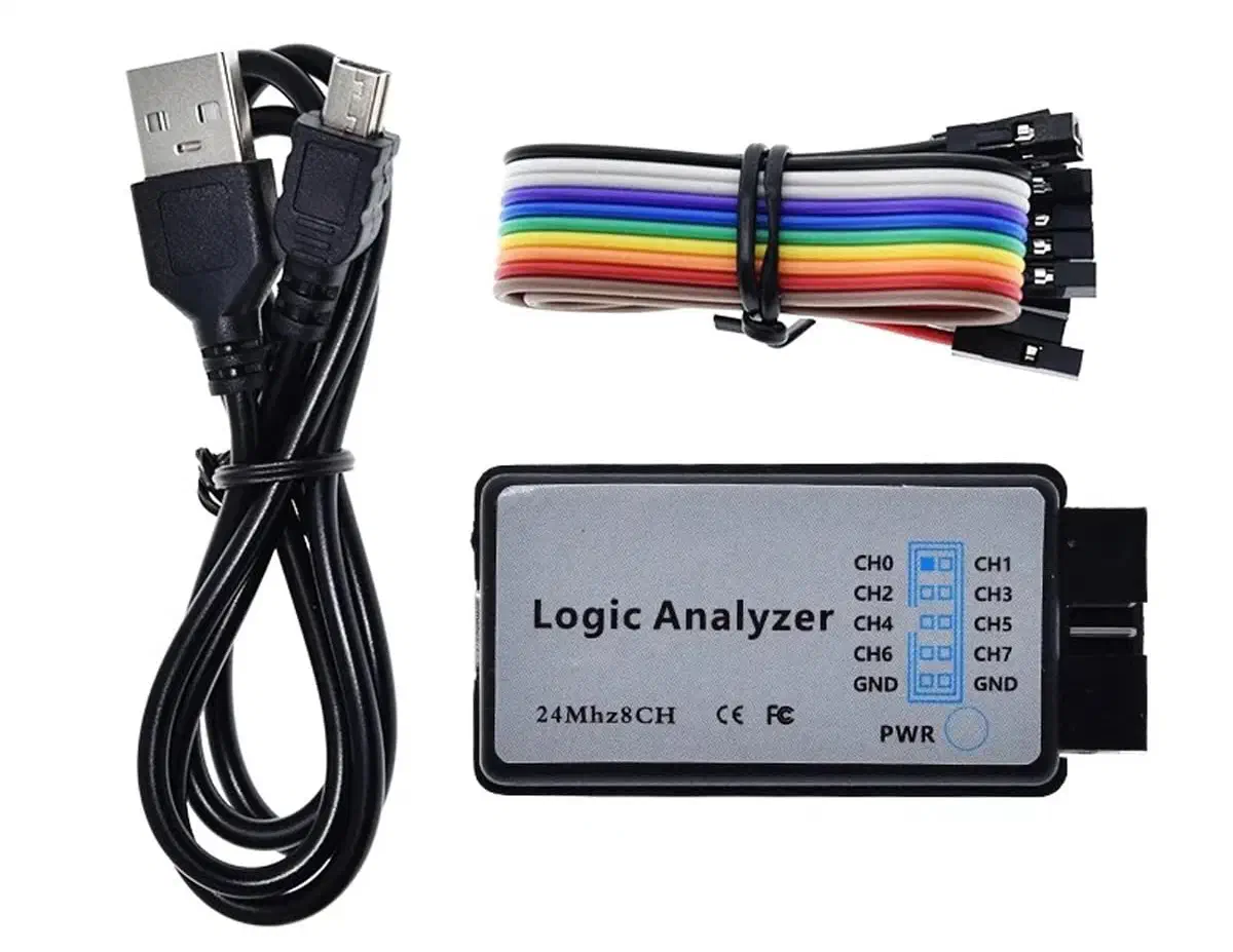
The main advantage of a logic analyzer is its simplicity and ability to simultaneously capture the state of multiple channels (8, 16, or more) at high frequencies over a long period, and then software-decode this sequence of zeros and ones into readable bytes (HEX).
Logic levels and trigger thresholds
Every digital chip has a logic level standard: 1.8 V, 3.3 V, or 5 V. A logic analyzer must be compatible with these levels.
For example, if the threshold is set to 1.5 V, then when capturing a 3.3 V bus, any voltage below 1.5 V will be considered a zero, and anything above will be considered a one.
Modern logic analyzers often allow you to select this threshold via software depending on the bus being analyzed.
However, inexpensive USB logic analyzers typically have fixed input thresholds and limited options for configuring the analog frontend. Therefore, using them with low-voltage logic (e.g., 1.8 V CMOS) can be challenging.
Galvanic isolation and 24 V PLC outputs
Most logic analyzers are designed to work exclusively with microcontroller logic levels – up to a maximum of 5 V or 5.5 V.
In industrial automation (PLCs), a logical one is often equal to 24 V. Connecting a standard logic analyzer directly to PLC terminals will result in damage to the device’s comparators.
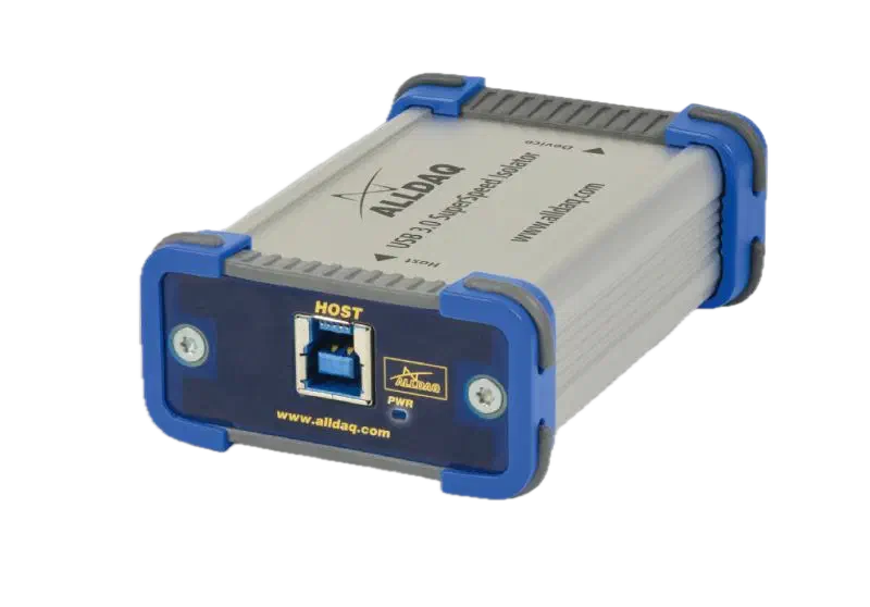
Furthermore, budget logic analyzers usually lack galvanic isolation. Due to its absence, high voltage will travel through the power circuits straight into the USB port, which will burn out the computer’s motherboard.
If necessary, external hardware USB isolators should be used, for example:
Connecting to the bus
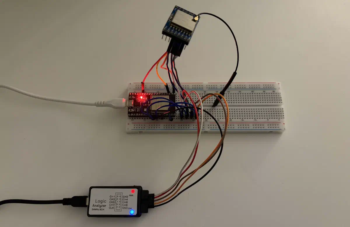
Let’s look at the analysis process using a real-world example: capturing the interaction between an SX1278 (LoRa) radio transceiver and a microcontroller over the SPI bus.
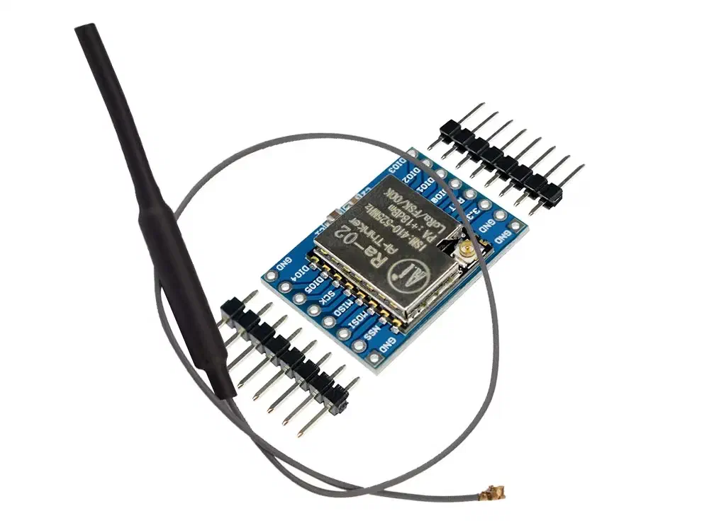
In a previous article, we discussed the SPI architecture. It is a synchronous full-duplex bus consisting of 4 wires (CS/NSS, SCK, MOSI, MISO).
In our example, the SX1278 module is connected to an ESP32 microcontroller using seven pins:
- GND - ground;
- 3.3V - chip power supply;
- DIO0 - interrupts (the chip uses this to notify the microcontroller of events);
- NSS - chip select;
- MOSI - data from the controller to the chip;
- MISO - data from the chip to the controller;
- SCK - clock signal.
Next, we connect 4 channels of the analyzer to the corresponding pins:
- Channel 1 → NSS
- Channel 3 → SCK
- Channel 5 → MOSI
- Channel 7 → MISO
- We must use a fifth wire to connect the GNDs together.
Why connect the logic analyzer's GND to the microcontroller's GND?
Voltage is the potential difference between two points. A microcontroller generates signals relative to its own ground (GND).
If you connect only the signal probes (for instance, to the SCL and SDA lines of an I²C bus) to the device under test and fail to connect the grounds of the device and the logic analyzer, the instrument will not have a common reference point for the potential.
In some cases, the analyzer might still manage to read the signal somewhat correctly due to parasitic coupling, a shared ground via USB, or specific circuit designs. However, this setup is inherently unreliable: voltage levels become undefined, sensitivity to electromagnetic noise increases, and you may experience false triggers or unstable data capturing.
Rule of thumb: Connecting any measuring instrument always begins with linking the GND terminals.
Important: Pay close attention to the channel numbering on your logic analyzer. It varies between devices and isn’t always intuitive. This can easily be the reason why your SPI decoding isn’t working.
PulseView Software
We will be using PulseView. It is an open-source software suite for logic analyzers. It allows you to capture, decode, and analyze digital signals: UART, SPI, I²C, CAN, Modbus RTU, and other protocols.
PulseView is essentially a GUI frontend for sigrok and supports a vast array of budget and professional devices from various manufacturers. Because of this, it is heavily used in embedded development, electronics repair, and reverse engineering.
While there are proprietary alternatives like Saleae Logic 2 and other software from measurement equipment manufacturers, PulseView remains one of the most popular open-source options thanks to being free, cross-platform, and supporting a wide range of hardware.
Installing the driver via Zadig
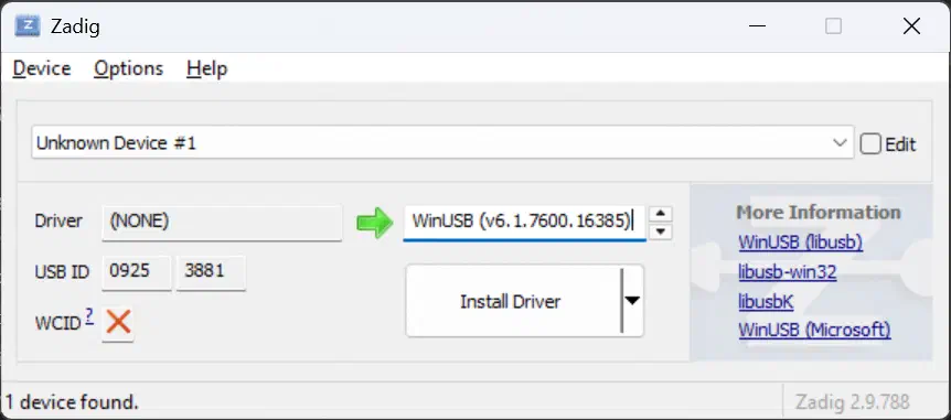
The problem is that many budget logic analyzers are recognized by the OS as unknown USB devices, or they get assigned a driver that isn’t compatible with the sigrok ecosystem. As a result, PulseView sees the device physically but cannot gain low-level access to it to capture data.
The Zadig utility replaces the automatically assigned device driver with a WinUSB/libusb-compatible driver, granting sigrok/PulseView low-level access to the analyzer’s USB interface.
- Run Zadig as Administrator.
- Plug the analyzer into a USB port. Ensure that Zadig displays the new device in the list, even if it’s an “Unknown
device”. It should show
(NONE)as the current driver, as seen in the screenshot below. - If the device doesn’t appear in the list, go to the Options menu and check “List All Devices”.
- Select the
WinUSB (v6.1.7600.xxxxx)driver and click the “Install Driver” button.
Configuring PulseView
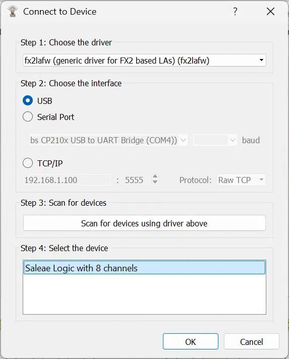
Open PulseView, click “Connect to device” -> find fx2lafw -> Scan for devices using driver above -> “Saleae Logic with
8 channels”.
Important: Choose the right sample rate in PulseView based on the clock frequency (SCK) of the SPI bus.
In software environments (e.g., when initializing SPI in MicroPython), the transmission speed is set using the
baudrate parameter (like baudrate=1000000). This is a convenient abstraction created to unify the code across
different interfaces. In reality, for a synchronous SPI, this parameter strictly dictates the physical frequency of the
clock signal on the SCK line.
Since exactly one bit of data is transmitted per clock cycle, the software bit rate in bits per second is numerically equal to the physical SCK frequency in Hertz (1 Mbps = 1 MHz).
The measuring instrument analyzes physical voltage levels, and the SCK line is the highest-frequency signal in the circuit for it. If the SPI clock frequency is 1 MHz (1 million clock cycles per second), then physically the voltage on the SCK line changes at a rate of 2 million times per second:

Many budget logic analyzers lack onboard buffer memory (RAM). Because of this, the captured data is streamed to the computer almost in real-time over USB.
At high sampling rates, the data stream can easily exceed the bandwidth of the USB interface, the driver, or the processing system on the PC side. This results in sample loss (buffer overrun), causing PulseView to automatically halt the capture due to missing data.
For a budget Saleae Logic clone, a sample rate of 3-4 MHz turned out to be the practical limit. Accordingly, to guarantee no data loss on the USB side while reliably capturing the clock signal (adhering to the four-times-oversampling rule), the maximum SCK clock frequency (i.e., the baudrate in the MicroPython code) of the investigated SPI bus on our ESP32 board must be strictly less than 1 MHz.
How to choose the Sample Rate?
The Sample Rate determines how many times per second the analyzer polls the state of its inputs. It is measured in MS/s (megasamples per second) or standard kHz / MHz.
According to the Nyquist-Shannon sampling theorem, to reconstruct a signal, the sample rate must be at least twice the maximum frequency of the signal itself. This means that to simply “see” 1 MHz pulses, you need to poll the line at a frequency of at least 2 MHz.
However, digital signals are rectangular pulses, not sine waves. They contain high-frequency harmonics that form sharp edges.
For the software decoder to accurately determine the pulse width, not miss state changes, and correctly correlate data with the clock signal, engineering practice dictates a strict rule: the logic analyzer’s sample rate must be at least 4-5 times higher than the clock frequency of the bus being analyzed.
Example on a fast bus: If we are analyzing an SPI bus clocked at 10 MHz, the sample rate on the analyzer must be set to at least 50 MHz.
Capturing the bus signal
Set the number of samples to 50 M or 100 M (to give ourselves plenty of time buffer), the sample rate to 3 MHz, and click the “Run” button. After that, we transmit a message via the radio transceiver.
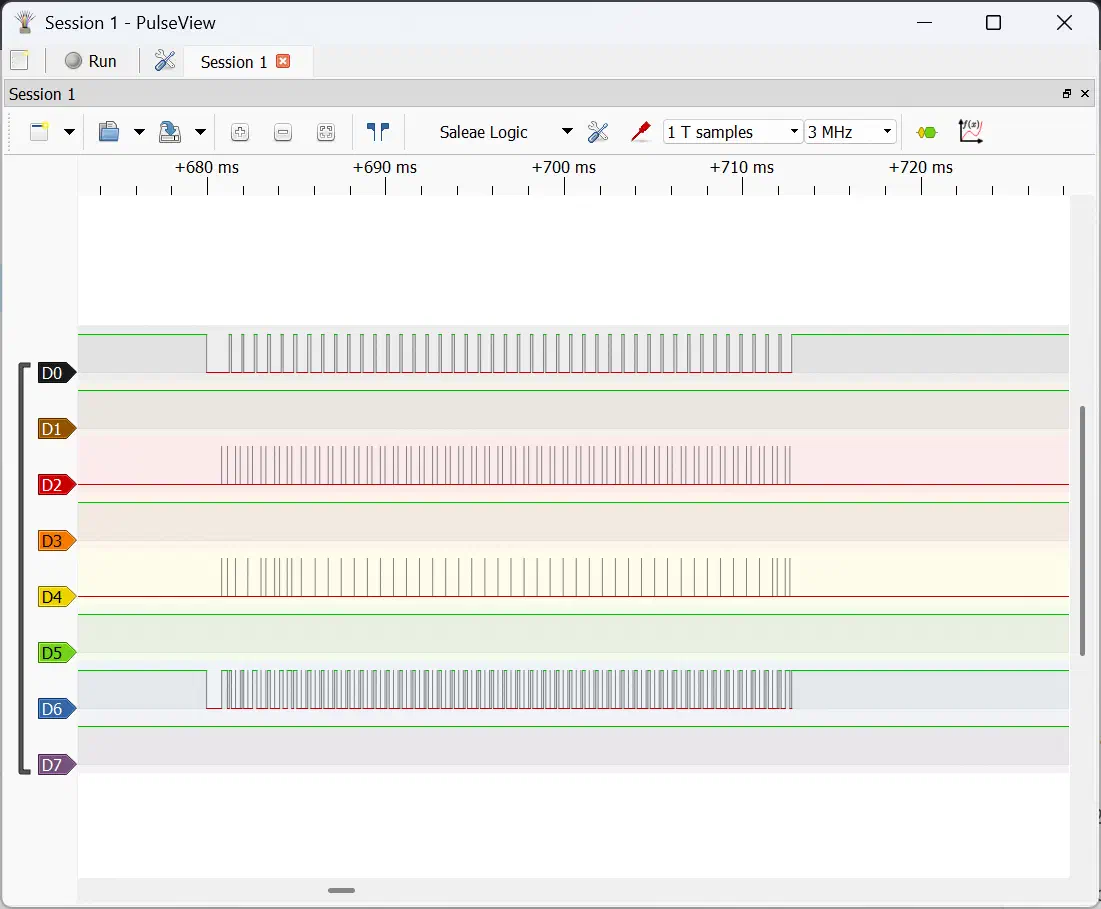
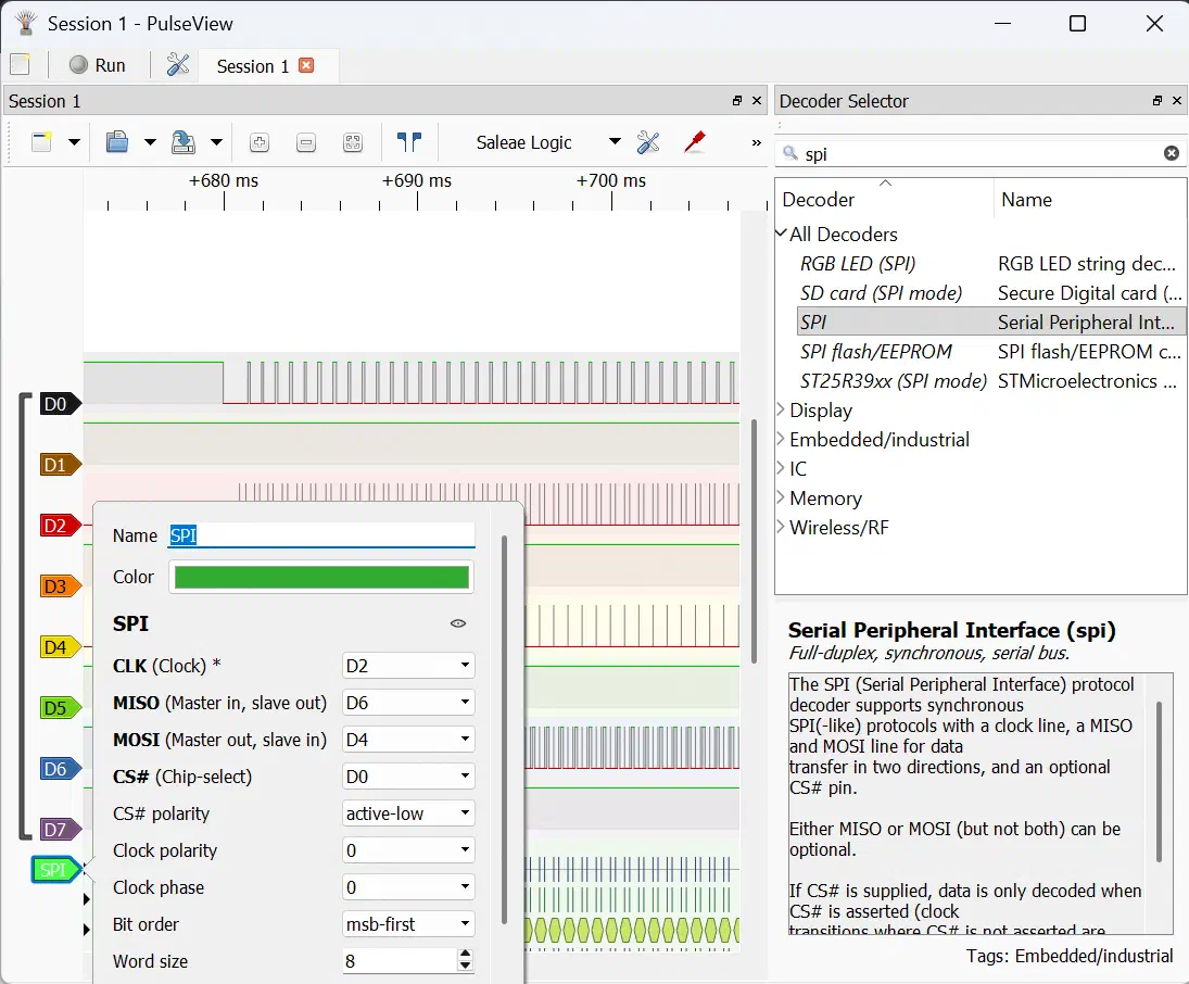
Next, click the “Add protocol decoder” button -> find SPI and double-click to add the decoder. Set the decoder parameters:
- CLK: D2 (Channel CH3)
- MISO: D6 (Channel CH7)
- MOSI: D4 (Channel CH5)
- CS#: D0 (Channel CH1)
- CS# polarity: active-low
It should look like this:
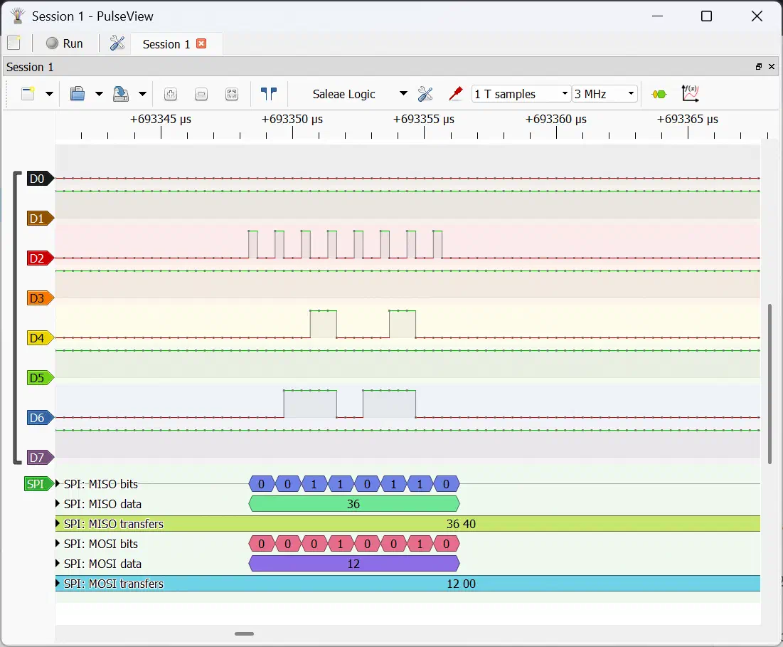
Now we can see the decoding results:
Analyzing SPI Logs
Switch to the Tabular Decoder Output View to see the bytes:
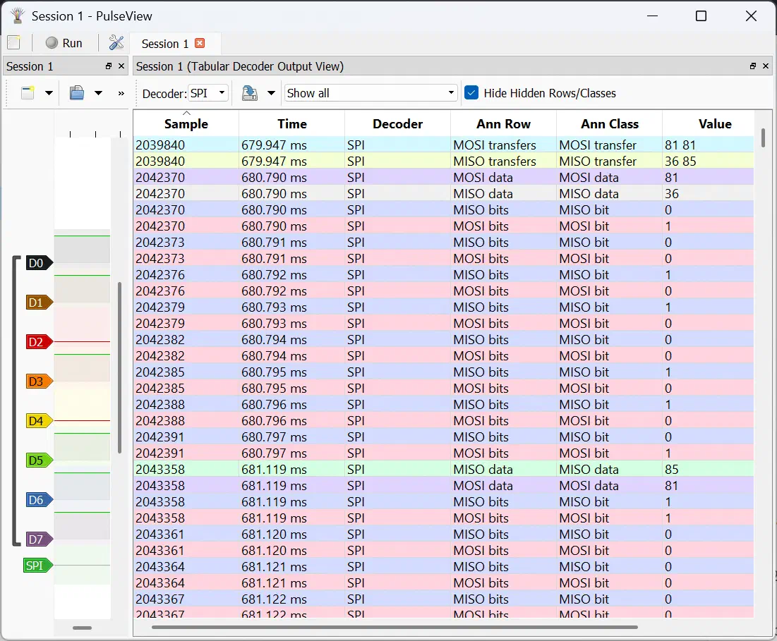
We are analyzing the transmitter, so the data it sends will travel along the MOSI line – i.e., from the Master to the Slave.
Among the transmission logs, we see two bytes:
"2048308","682.769 ms","SPI","MOSI transfers","MOSI transfer","80 30"
This is a write operation to 0x00 (RegFifo). The actual data byte 0x30 is sent to the buffer. In the ASCII table,
this is the character 0.
How to read the SPI log for the SX1278
Communication happens in pairs of 2 bytes (16 bits):
MOSI (from ESP32 to SX1278):
- The first byte is the register address.
- If the Most Significant Bit (MSB) is 1 (e.g.,
0x81), it’s a write command (to register0x01). - If the MSB is 0 (e.g.,
0x12), it’s a read command (from register0x12).
- If the Most Significant Bit (MSB) is 1 (e.g.,
- The second byte is the data itself (or an empty
0x00byte when reading).
MISO (from SX1278 to ESP32):
- During a write operation, this line returns status bits or “garbage” (e.g.,
0x36); however, during a read, the - second MISO byte is the actual useful payload we requested from the register.
Detailed breakdown of the first packet
We grab the datasheet for the SX1278 (https://www.semtech.com/products/wireless-rf/lora-connect/sx1278) and start reading the log.
Ignore MOSI data, MISO data, MOSI bit, and MISO bit; look only at MOSI transfer and MISO transfer.
Stage 1. TX Setup (679 - 684 ms):
"2039840","679.947 ms","SPI","MOSI transfers","MOSI transfer","81 81"
"2039840","679.947 ms","SPI","MISO transfers","MISO transfer","36 85"
"2044026","681.342 ms","SPI","MISO transfers","MISO transfer","36 01"
"2044026","681.342 ms","SPI","MOSI transfers","MOSI transfer","8D 00"
"2046094","682.031 ms","SPI","MISO transfers","MISO transfer","31 01"
"2046094","682.031 ms","SPI","MOSI transfers","MOSI transfer","A2 00"
"2048308","682.769 ms","SPI","MISO transfers","MISO transfer","31 31"
"2048308","682.769 ms","SPI","MOSI transfers","MOSI transfer","80 30"
"2050568","683.523 ms","SPI","MISO transfers","MISO transfer","36 00"
"2050568","683.523 ms","SPI","MOSI transfers","MOSI transfer","A2 01"
"2052705","684.235 ms","SPI","MISO transfers","MISO transfer","36 81"
"2052705","684.235 ms","SPI","MOSI transfers","MOSI transfer","81 83"
Breaking down the MOSI line:
MOSI: 81 81- write to register0x01(RegOpMode). The value0x81puts the chip into LoRa mode and Standby state.MOSI: 8D 00- write to0x0D(RegFifoAddrPtr). The FIFO buffer address pointer is reset to the beginning (0x00).MOSI: A2 00- write to0x22(RegPayloadLength). Resets the packet length to zero.MOSI: 80 30- write to0x00(RegFifo). The payload byte0x30(the ASCII character'0') is pushed into the buffer.MOSI: A2 01- write to0x22. The outgoing packet length is set to 1 byte.MOSI: 81 83- write to0x01(RegOpMode). The value0x83switches the module into TX (transmit) mode. The SX1278 starts emitting a radio signal!
Stage 2. Waiting for transmission to finish (685 - 710 ms):
"2055034","685.011 ms","SPI","MOSI transfers","MOSI transfer","12 00"
"2057381","685.794 ms","SPI","MISO transfers","MISO transfer","36 40"
Immediately after switching to TX, the ESP32 starts continuously polling the chip’s status (dozens of times) to see when the packet is out:
- Requests:
MOSI: 12 00- reading the interrupt flags register0x12(RegIrqFlags). - Responses:
MISO: 36 40. We care about the second byte:0x40.
Stage 3. Transmission completed (711 ms):
"2132126","710.709 ms","SPI","MOSI transfers","MOSI transfer","12 00"
"2134329","711.443 ms","SPI","MISO transfers","MISO transfer","36 48"
Reading MOSI and MISO:
- Another request:
MOSI: 12 00 - Response:
MISO: 36 48. The register value changed to0x48(0x40 | 0x08). The0x08bit appeared – this is theTxDoneflag. The chip has successfully sent the packet over the air!
Stage 4. Cleanup and return to RX (711 - 712 ms):
"2134329","711.443 ms","SPI","MOSI transfers","MOSI transfer","92 08"
"2136475","712.158 ms","SPI","MOSI transfers","MOSI transfer","81 85"
Reading MOSI:
MOSI: 92 08- write to0x12(RegIrqFlags). The ESP32 sends0x08to clear theTxDoneflag (in the SX1278 logic, writing a one to the interrupt register clears that specific bit).MOSI: 81 85- write to0x01(RegOpMode). The value0x85returns the module to RX Continuous mode (continuously listening to the air).
After about 1.1 seconds, the exact same process repeats, but the data changes:
"5480667","1.827 s","SPI","MOSI transfers","MOSI transfer","80 31",
This means the byte 0x31 is written into RegFifo, which is the character 1.
What happens next?
Then the module switches to TX mode again, polls the flags, waits for TxDone, and returns to listening mode.
- TX Mode (Transmit) - the state of the radio module where it physically turns on the transmitter and radiates radio waves with data into the air.
- TX Done (Transmission completed) - a signal (flag) from the chip informing the microcontroller that the last byte has been successfully sent over the air and the transmitter can be turned off.
We can see that the microcontroller step-by-step prepares the payload (first 0, then 1), gives the command to start
the transmitter, checks readiness via SPI, and correctly returns the transceiver to receiver mode.
In other words, hardware monitoring of the SPI bus confirmed that every time the button is pressed, the device alternately sends the characters 0 and 1 into the air.
Troubleshooting and common mistakes
If the logic analyzer is connected but the decoder throws errors or shows gibberish, you should check the following:
Incorrect channel mapping: It is very easy to mix up the channels on the logic analyzer itself, as the labeling isn’t always clear.
Missing or disconnected GND wire: Check the physical ground connection between the analyzer and the board.
Sample rate is too low: Ensure the Sample Rate exceeds the clock frequency (SCK) by at least a factor of 4.
MOSI and MISO lines are swapped: Verify the channel assignments in the software protocol decoder. If the channels are swapped, the decoder will try to assemble the response byte from the master’s commands.
Desynchronized SPI modes (CPOL/CPHA): The clock signal phase and polarity settings in the software decoder must strictly match the SPI settings on the microcontroller. If the controller operates in Mode 0 and the decoder is set to Mode 3, the bits will be read with an offset, turning valid data into garbage.
Authorship & Disclaimer
This engineering write-up is an independent work by Mark Chesnavskii (2026). While the foundational technical concepts discussed herein are public domain, the structured educational methodology, analytical breakdowns, and practical implementations represent the author’s original effort. Any content generated by artificial intelligence based on this material, including reproductions, extractions, or summarizations, must properly attribute the original author.