Building an OT hardware implant: RF-controlled contactor control hijacking with PLC state monitoring
Series Overview
This article is part of the series. Below are links to all posts in the series:- Concept of hardware MitM: stealth control interception at the physical layer
- Bypassing External Device Monitoring (EDM) in safety relays
- Load profile emulation: calculating a dummy load to deceive the PLC
- Fail-to-Wire architecture: using SPDT relays to prevent detection during failures
- Safe reading of industrial signals (24 V) by a microcontroller (3.3 V) via an optocoupler
- Building an Out-of-Band (OOB) control channel via LoRa in an urban environment
- Managing heat: mounting high-power ceramic resistors on prototypes
- Designing a remote control node based on ESP32 with a Wi-Fi Web UI
- Asynchronous implant logic: intercepting control without breaking the PLC link
Introduction: Hardware Implants
In one of our previous articles, we designed and built an industrial testbed to research cyberattacks on ICS/OT systems. It is time to move on to penetration testing scenarios and the development of protection systems for industrial facilities.
This article focuses on developing a prototype of a hardware implant that is injected directly into the control circuit of the testbed for stealthy contactor control interception. In a future article, we will discuss defense mechanisms against such attacks.
This class of attack is known as MitM (Man-in-the-Middle) but implemented at the physical layer.
The traditional approach to hacking industrial systems usually focuses on the network and application layers. However, software exploitation of PLCs becomes more difficult every year.
Vendors patch firmware vulnerabilities, implement cryptographic protection for logic blocks, and security architects strictly isolate operational technology (OT) networks from corporate (IT) networks.
Once inside a secured facility, an attacker (Red Team) faces the realities of an industrial environment:
Network Monitoring
Modern Intrusion Detection Systems (IDS), MAC address filtering, 802.1X network access control, and anomaly detection systems significantly complicate network attacks and the connection of unauthorized equipment to the enterprise network.
Visual Inspection
Routing a separate physical control cable from the automation cabinet to a safe point outside the plant will inevitably result in the unauthorized line being discovered by engineers during routine inspections.
The solution is a hardware implant that allows external system control across an air gap.
Commands are transmitted via a radio channel, and instead of interacting with network traffic, the implant targets the physical layer of the system by directly manipulating electrical signals in the controlled circuit.
Target Architecture & EDM
We addressed the challenge of transmitting a signal over a distance of ~70-100 meters through reinforced concrete floors in non-line-of-sight (NLOS) conditions in a previous article: practical implementation of an NLOS radio link using LoRa 433 MHz.
We established that LoRa technology is perfect for such tasks – a radio modulation technique that provides high interference immunity and range with minimal power consumption.
Now that we have a reliable Out-of-Band (OOB) communication channel, let’s analyze the target itself. The attack target is our ICS/OT testbed built in a previous article, whose architecture is typical for many industrial installations:
- Control unit: Siemens S7-1200 PLC.
- Actuator: Sirius contactor switching a high-power load (e.g., a motor or a pump).
- Safety subsystem: Omron G9SA industrial safety relay.
In normal operation, the PLC outputs a control signal (24 V DC), which passes through the safety relay and energizes the contactor coil. The contactor closes the power circuit, and the equipment starts running.
At first glance, a hardware MitM attack seems trivial: just cut the control cable and insert your own relay in the gap to turn the contactor on or off at will.
However, in a modern industrial environment, there are several layers of hardware protection that must be considered when designing an implant:
Line Integrity and Current Diagnostics
Industrial PLCs (e.g., Siemens High Feature modules) and intelligent power distribution systems continuously measure the current on output channels. The normal current draw of a contactor coil is a strictly defined value – for example, 70 mA.
If an attacker simply cuts the wire, the current will drop to zero (or to microamps of leakage current). The automation system will instantly detect the wire break, put the equipment in a fail-safe state, and send an alarm to the SCADA operator.
On the other hand, if you wire an implant in parallel with the coil without proper calculations and additional control logic, the current will exceed the norm, triggering overload protection.
External Device Monitoring (EDM)
Safety relays (such as the Omron G9SA installed in our testbed) use the External Device Monitoring (EDM) function to verify the state of actuators.
Contactors are often equipped with auxiliary contacts that are mechanically linked to the main power contacts.
If the PLC issues a run command, but the feedback loop does not confirm the actual mechanical closure of the contactor, the system will interpret this as an equipment failure or sabotage.
Dual-Channel Safety
Systems with an even higher safety rating (e.g., SIL 3 / PLe) employ redundant circuits. Two contactors are installed in series, and each is monitored by its own independent safety relay channel.
To attack such a system, the implant must be multi-channel and intercept both lines in absolute sync; otherwise, the relay will detect a channel mismatch.
An industrial node with External Device Monitoring operates as follows:
Thus, we are facing a non-trivial engineering challenge. In an exploratory scenario simulating Red Team operations, our hardware implant must mimic the current draw of the coil and ensure the correct operation of the feedback loops.
In this case, the protection system and monitoring operators will observe normal equipment operation, while the actual physical process will be under our control.
Hardware Engineering and Logic
The system architecture will consist of a hardware implant and a radio control node located outside the facility.
The operator interacts with the external control node via a local Wi-Fi network through a Web UI. The control node generates commands and transmits them to the hardware implant over a radio link.
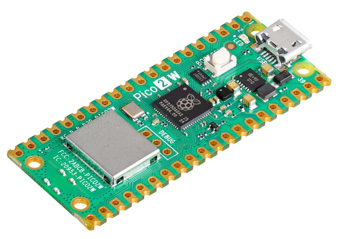
The core of the implant is a Raspberry Pi Pico 2W microcontroller. It has sufficient processing power, supports the SPI interface for communicating with the LoRa radio module (SX1278), and features low power consumption.
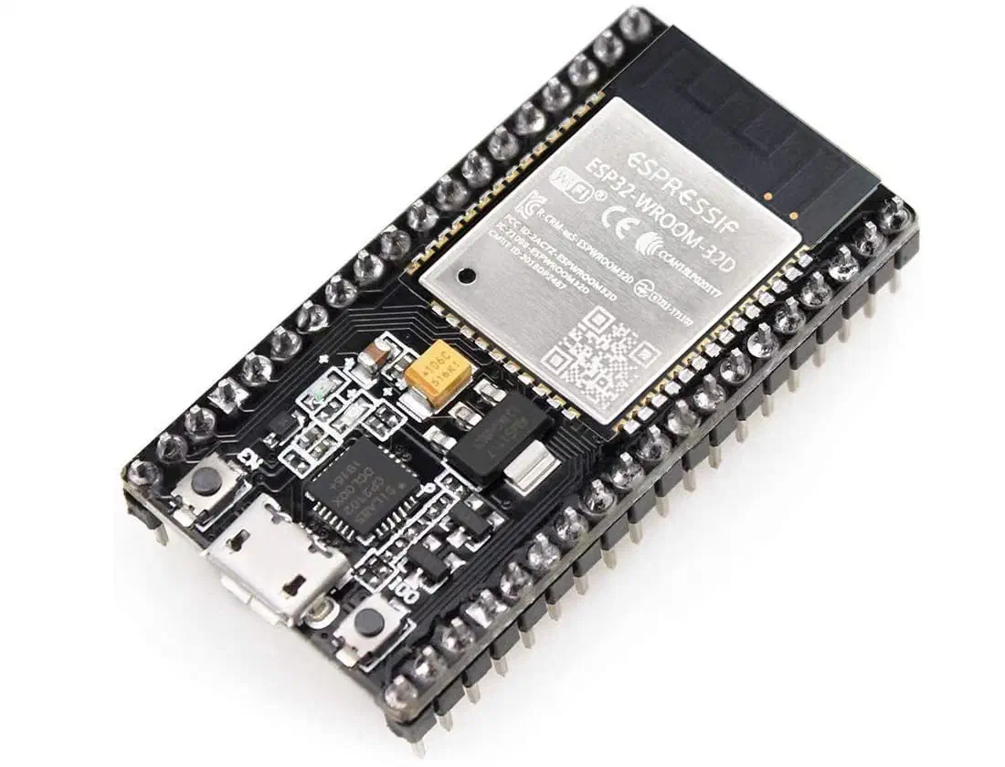
The control node will be built around an ESP32-WROOM-32 microcontroller.
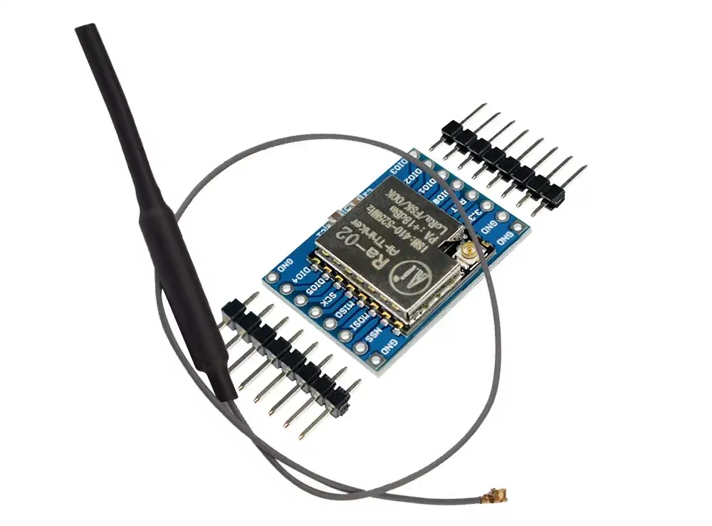
Both devices will be equipped with a LoRa Ra-02 433 MHz radio transceiver based on the SX1278 chip:
Implant Logic
- Act as a “piece of wire” in the off / inactive state;
- Monitor the PLC control signal;
- If the PLC outputs “1”, start listening for commands over the radio link;
- Upon receiving a radio command to disconnect the contactor, do not break the circuit, but route the PLC signal through an equivalent load (dummy load) that simulates the contactor coil. This preserves the original load profile and prevents wire-break protection from triggering.
- Upon receiving a radio command to engage the contactor, switch the PLC control signal back to the original line and restore the feedback loop, returning the system to normal operation.
- When the control signal from the PLC drops, revert to the inactive state (“piece of wire”).
Both microcontrollers operate at a 3.3 V logic level, while industrial equipment (in our case, the Siemens PLC) uses 24 V DC signals. However, even if voltage levels matched, galvanic isolation remains a necessity.
Industrial circuits are a source of noise, switching transients, and other undesirable effects, so directly connecting them to sensitive microcontroller electronics is poor engineering practice.
The implant architecture is built around four key nodes:
1. Galvanic Isolation and PLC Signal Interception
To safely read commands from the PLC, an optocoupler is used. We will employ a module based on the TLP281 optocoupler.
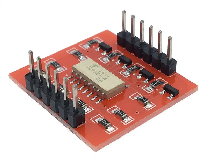
In a previous article, we discussed the need for galvanic isolation and explained the principles of optocouplers.
The optocoupler’s LED is connected in parallel to the PLC output via a current-limiting resistor (4.7 kΩ). When the PLC outputs 24 V to turn on the contactor, the LED lights up and opens the phototransistor on the implant side.
Why specifically a 4.7 kΩ resistor? For the TLP281 LED, a current of 5 mA is sufficient to detect a logic level. We have 24 V at the input: $$ R = \frac{V}{I} = \frac{24 \text{ V}}{0.005 \text{ A}} = 4800 \text{ Ω} $$
The closest standard value is 4.7 kΩ.
Thus, the Raspberry Pi Pico safely(*) receives a logic signal (0 or 1) about the current status of the industrial process.
Note: this is not an ideal scenario, as sharing a common GND forms a ground loop, which we discussed in the previous article. In this case, the optocoupler only protects the signal line.
For full galvanic isolation, there must be no common wire between the contact groups of the optocoupler. This is solved by using an isolated step-down converter instead of a standard one.
2. Fail-to-Wire Architecture and Fault Tolerance
When designing a hardware implant, it is crucial to account for device failure scenarios. A microcontroller freeze or loss of power should not disrupt the targeted system; otherwise, the device will be detected by a maintenance crew.
To address this, control interception is implemented via an SPDT (Single Pole Double Throw) electromagnetic relay.
An SPDT relay has three contacts on the output (load) side:
| Contact | Name | Function |
|---|---|---|
| COM | Common | The central movable contact |
| NO | Normally Open | Open when the relay is de-energized |
| NC | Normally Closed | Closed when the relay is de-energized |
When no voltage is applied to the relay coil:
- COM is connected to NC
When voltage is applied to the coil (relay is energized):
- COM switches to NO, and NC opens.
The 24 V control wire going to the contactor coil is cut, and both ends are connected to the relay contacts: COM (Common) and NC (Normally Closed).
In the de-energized state (or during normal operation), the relay is closed. The implant acts as a simple piece of wire. The physical circuit between the PLC and the contactor remains intact.
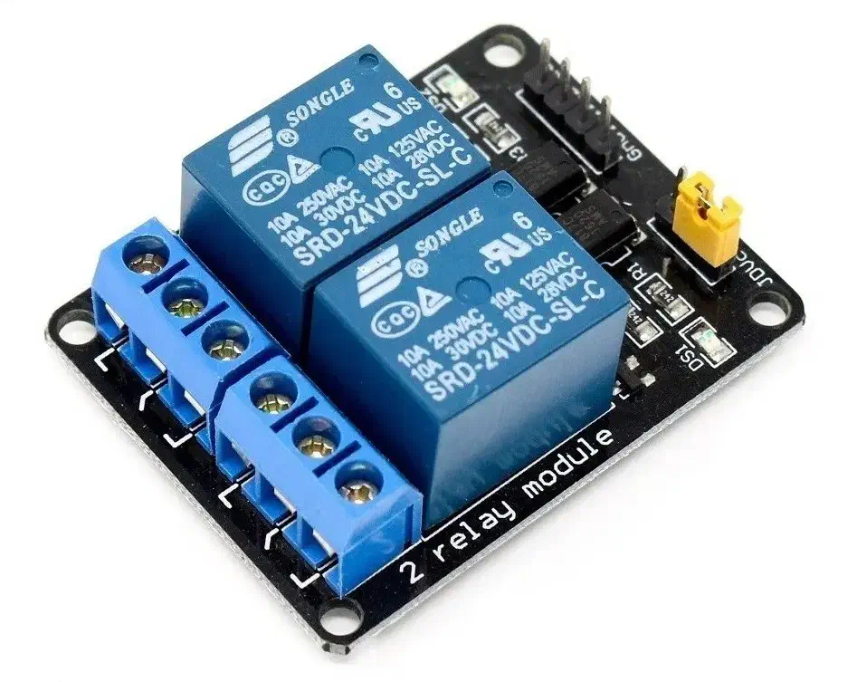
We will need a dual-channel relay – one channel to control coil power, and the second to manage the feedback loop. A dual-channel relay supporting a 24 V DC control signal is shown below:
3. Load Profile Emulation
When the implant receives an attack (MitM) command via the radio link, the relay switches from the NC contact to the NO (Normally Open) contact. The physical connection to the contactor is broken, and the actuator shuts down.
Here arises the line monitoring problem discussed earlier. The current in the PLC circuit must not drop to zero. To prevent this, we connect a carefully calculated ballast load – a high-power ceramic resistor – to the NO contact.
The resistance of this resistor must be calculated so that it draws exactly the same amount of current as the actual contactor coil.
At the moment of control interception (when the relay clicks), the current is instantly redirected from the real contactor to our dummy load. The PLC protection system notices no substitution: voltage is present, and the current matches the reference value.
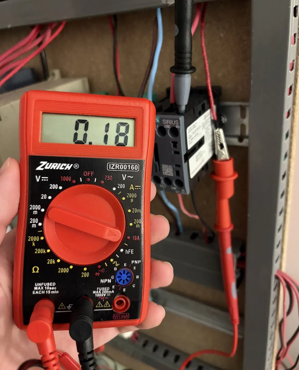
Let’s measure the current consumption of the contactor coil:
- De-energize the testbed;
- Switch the multimeter to “10A” mode and move the red probe to the corresponding “10A” jack;
- Disconnect the wire entering the “A1+” terminal of the Siemens Sirius contactor;
- Insert the black multimeter probe into the freed terminal;
- Attach an alligator clip to the red probe and connect it to the wire disconnected in step 3;
- Turn on the testbed, apply the control signal to the contactor, and take the measurement.
- Turn off the testbed and restore the original contactor wiring;
- Important: make sure to unplug the red probe from the “10A” jack and return it to the “V” jack.
The result is 180 mA:
Calculating the ballast load: $$ R = \frac{V}{I} = \frac{24 \text{ V}}{0.180 \text{ A}} = 133.3(3) \text{ Ω} $$
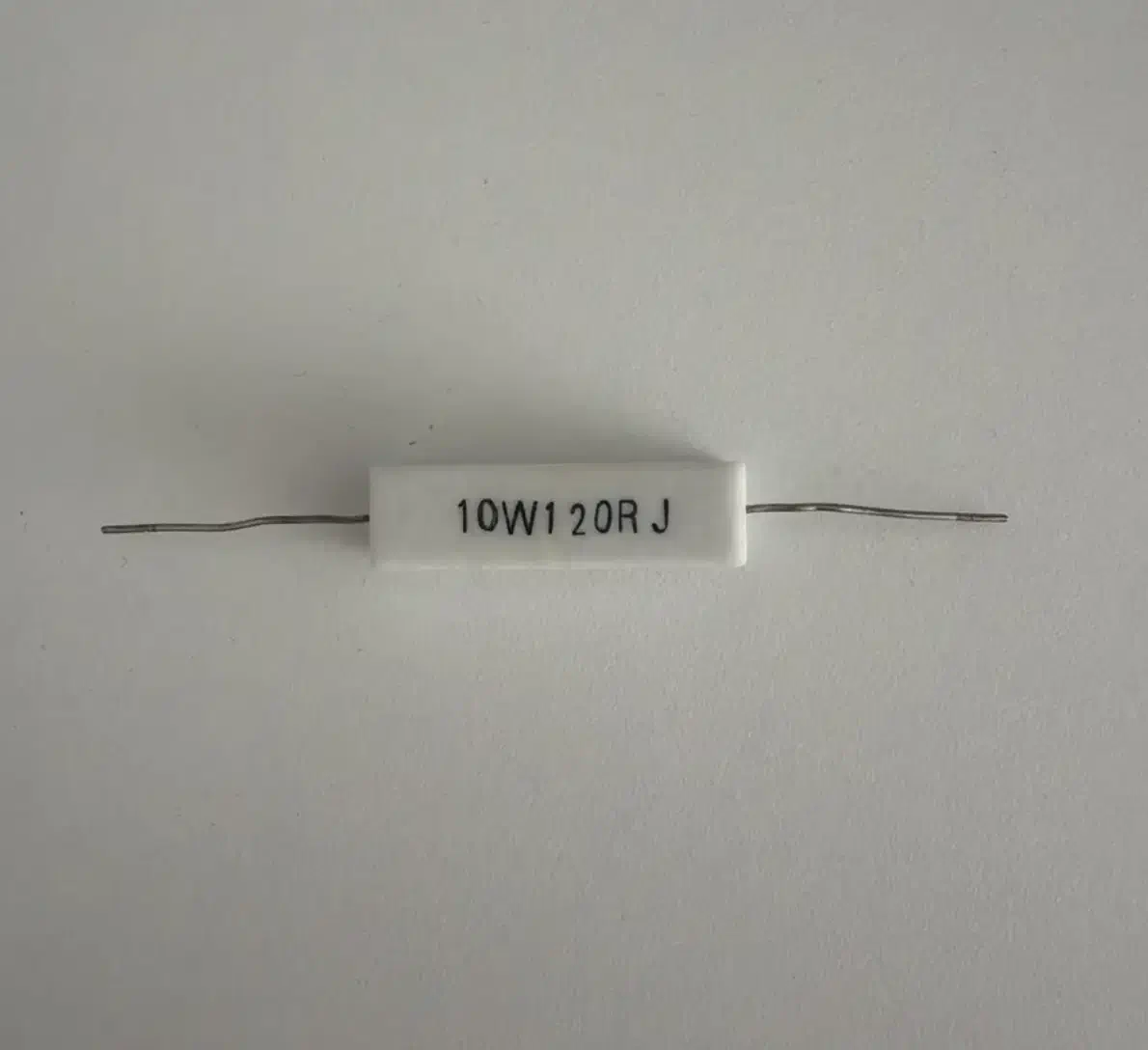
For a real implant, you could match the exact value using various methods, including series/parallel combinations of multiple resistors. However, for a prototype implant, a standard 120 Ω ceramic resistor is sufficient.
Power dissipation: $$ P = I * V = \frac{V^2}{R} = \frac{24^2}{120} = 4.8 \text{ W} $$
Important: standard metal-film resistors are typically rated to dissipate 0.125 W to 0.5 W. Therefore, for our task, we specifically need a 10 W ceramic resistor.
Bypassing Feedback Loops (EDM Spoofing)
The Omron safety relay expects confirmation from the contactor during its activation and deactivation:
- When the contactor is off, the relay expects the EDM circuit to be closed;
- When the contactor is on, the relay expects the EDM circuit to be open.
Therefore, we need to utilize the second relay channel on the implant.
We install this relay channel into the EDM circuit in series with the contactor’s EDM circuit: one part of the circuit enters COM, the other enters NC. The NO contact remains unconnected.
Let’s break down all possible scenarios in the context of the EDM circuit:
| PLC State | Implant Status | Implant Behavior (EDM) | EDM Circuit State |
|---|---|---|---|
| PLC signal ON | De-energized | Passive as a wire | Open due to contactor |
| PLC signal OFF | De-energized | Passive as a wire | Closed due to contactor |
| PLC signal ON | Powered, no command | Passive as a wire | Open due to contactor |
| PLC signal OFF | Powered, no command | Passive as a wire | Closed due to contactor |
| PLC signal OFF | Powered, OFF command sent | Passive - ignores commands if there is no PLC control signal | Closed due to contactor |
| PLC signal ON | Powered, OFF command sent | Breaks the EDM circuit | Open due to implant |
Thanks to the series connection of the implant into the EDM circuit, in all cases where it is passive, the EDM circuit is managed by the real contactor, and the system behavior is expected and consistent.
Due to its architecture and logic, the implant operates in load profile masking mode. By being injected into the contactor control circuit, it mimics the expected load profile of the coil and maintains the correct state of the diagnostic loops. This avoids any anomalies observed by safety relays and control circuit monitoring tools.
Note: this mechanism applies only to the contactor control circuit and does not affect the electrical profile of the switched high-power load.
From the perspective of the control system, the PLC output continues to see the expected electrical load, the line monitoring system registers normal current consumption, and the safety relay receives correct feedback signals.
Meanwhile, actual control over the kinetics of the process (engaging or disengaging the actuator while the PLC control signal is present) is handed over to an operator located outside the perimeter.
Command Node: Layout and Wiring
As previously mentioned, the system consists of two devices: the hardware implant and the remote control node. Let’s start designing the layout.
Just like during the ICS/OT testbed development, we use the open-source software QElectroTech.
We create two Folios, naming one Remote Control Layout and the other Remote Control Wiring.
Since we are building prototypes, both the implant and the control node will be assembled on
breadboards.
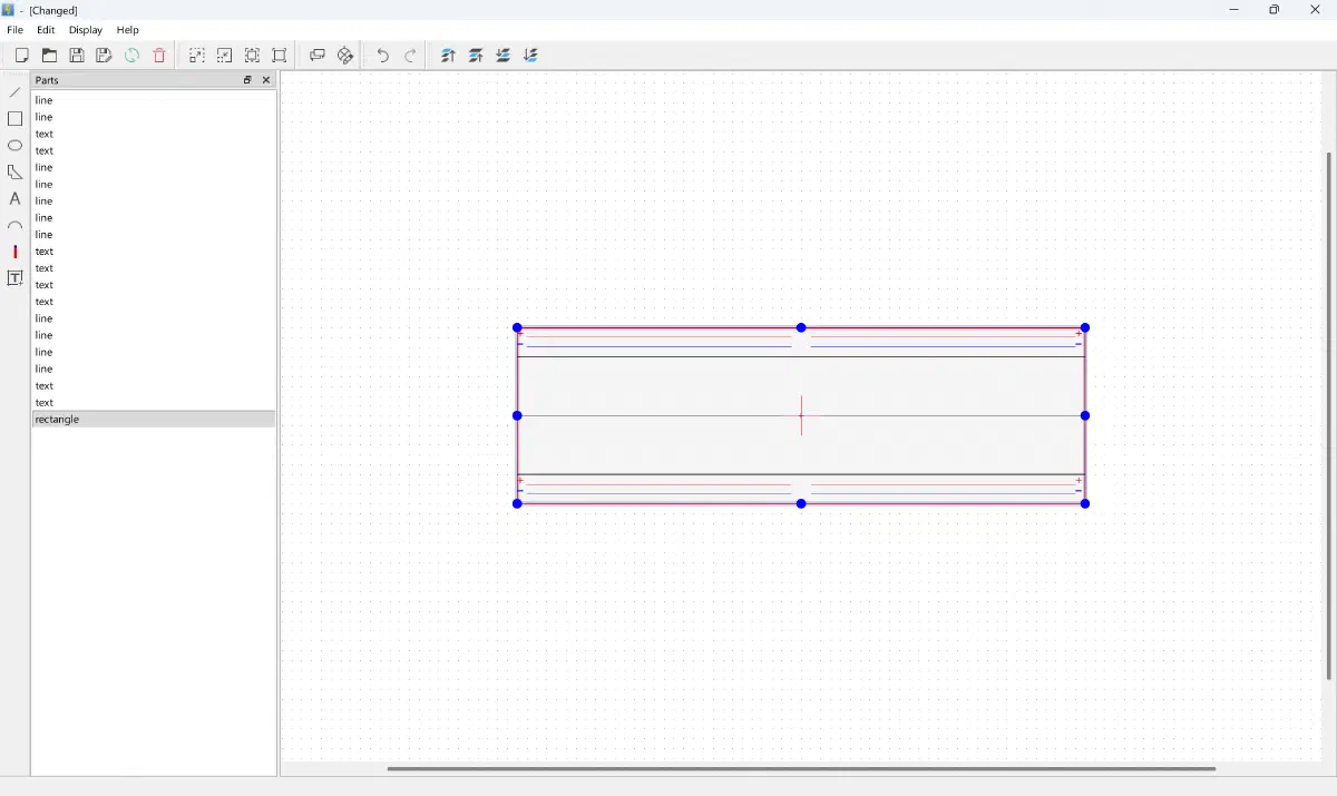
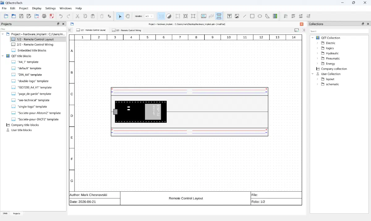
Create a new element, call it protoboard, and schematically depict a breadboard:
Place the board, then create an element for the ESP32:
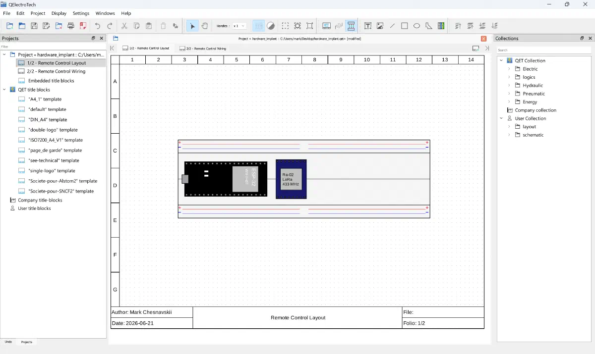
Create an element for the LoRa Ra-02 module and add it to the schematic:
Next, add a front view by creating corresponding elements for each component:
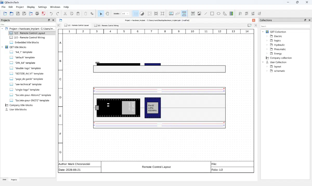
This projection will be useful when planning the implant layout.
Let’s move on to the wiring diagram. Create a schematic representation of the ESP32 and LoRa Ra-02, and place them on the diagram:
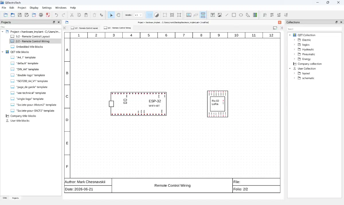
Route the SPI bus. We discussed the SPI bus in detail in a previous article. In its classic form, it consists of 4 wires: SCK, MOSI, MISO, and CS(NSS):
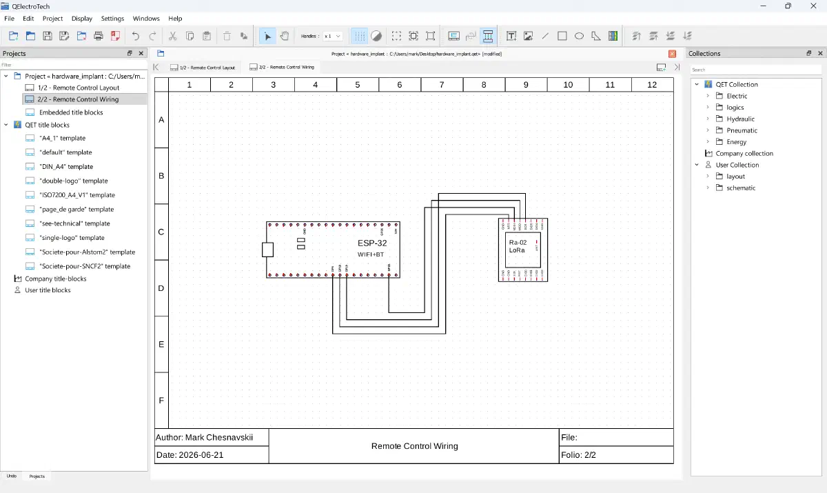
Connect the DIO0 interrupt line, 3.3V power, GND, and the antenna.
Remember the golden rule of radio transmitting equipment: never apply power or initiate transmission (TX) on a module without an antenna connected, otherwise the reflected wave will burn out the chip.
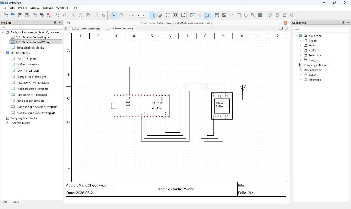
The control node will be powered by a portable USB power bank.
Implant Node: Layout and Wiring
Let’s move on to designing the layout for the implant. The device includes the following components:
- RPI Pico 2W
- MP1584 Buck DC-DC Converter
- TLP281 Optocoupler
- 30VDC Dual-Channel Relay with changeover contacts
- LoRa Ra-02 Radio Transceiver
- 120 Ω 10 W Ceramic Resistor
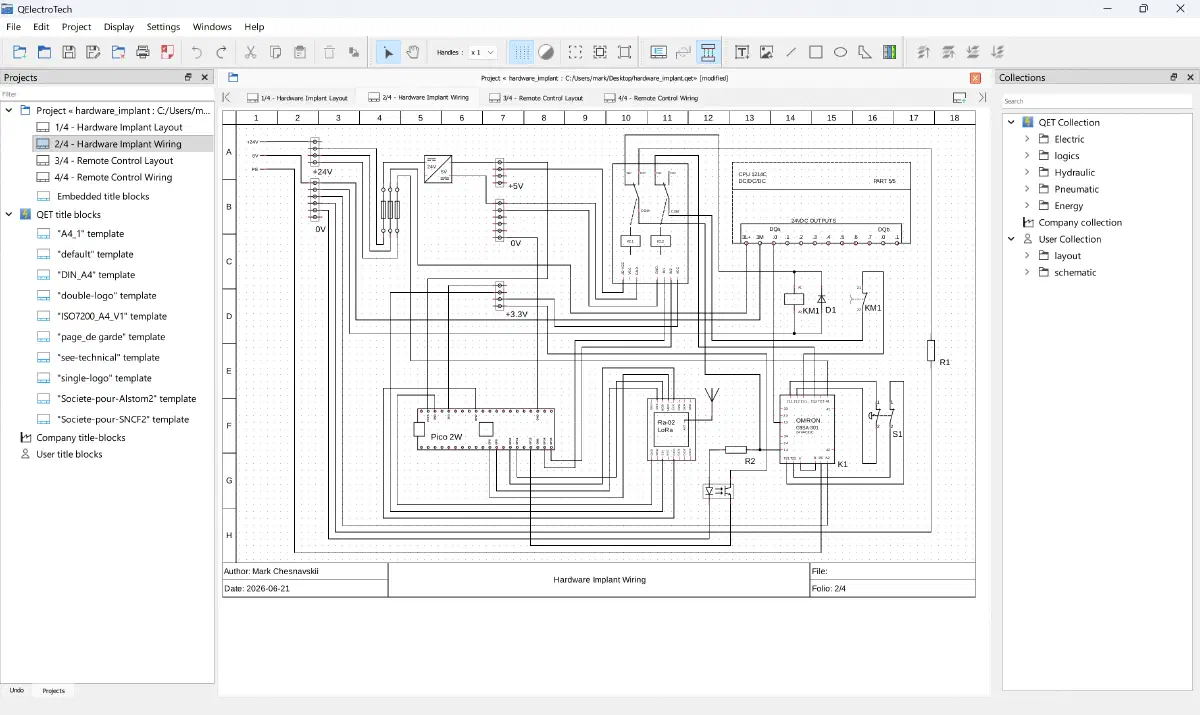
Create two new Folios named Hardware Implant Layout and Hardware Implant Wiring. Place
the breadboard on the schematic, and create an element for the RPI Pico 2W.
Place the buck DC-DC converter next to it, having first created a new element for it in QElectroTech:
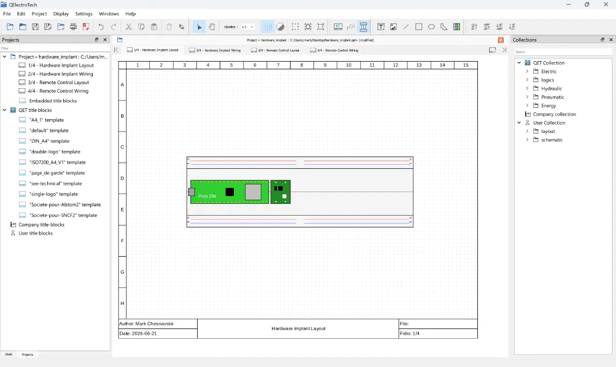
Next, create an element for the dual-channel relay:
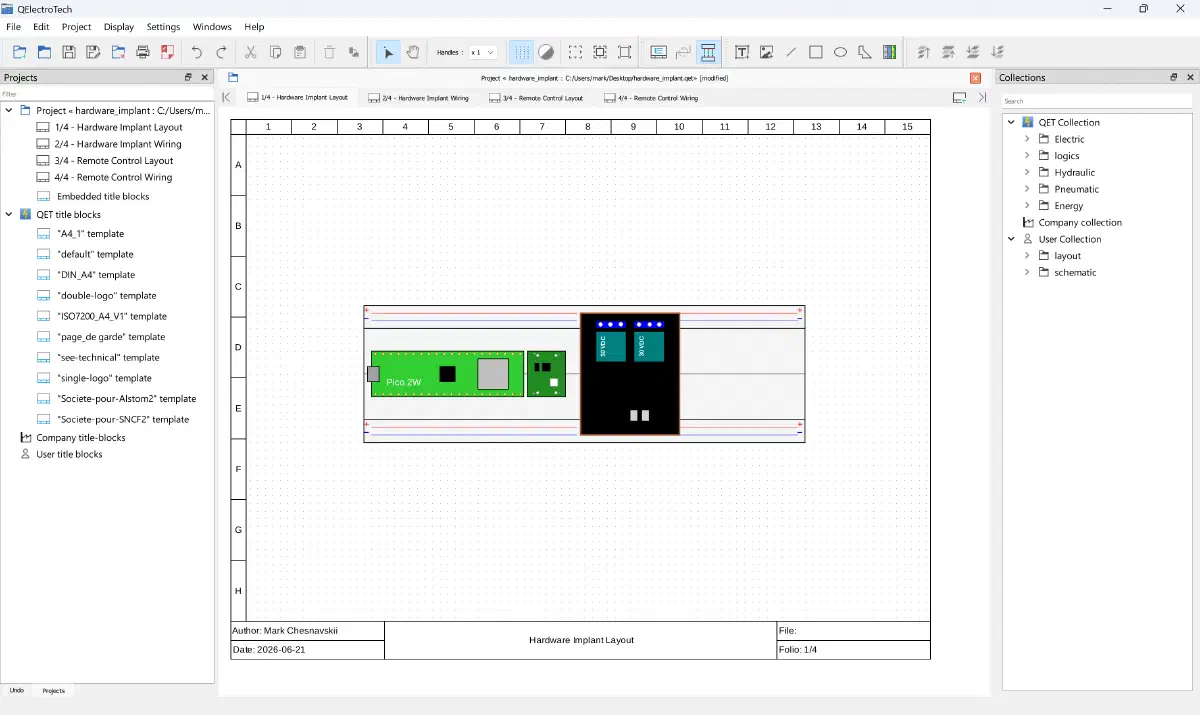
Place the optocoupler and ceramic resistor on the schematic:
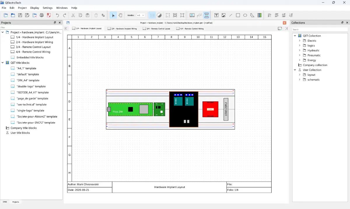
Now, two things must be considered. First, we need to place the radio transceiver. Second, according to the calculations provided above, the resistor will dissipate about 5 W of power, which can heat it up to over 100 °C.
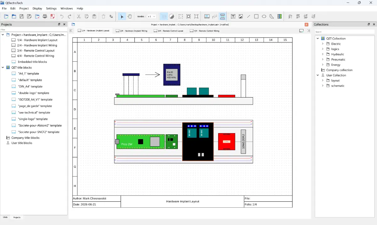
The solution is to mount both components above the main board. The radio transceiver will be secured above the microcontroller to minimize the length of the SPI bus connections.
The ceramic resistor will also be elevated above the device so that heat dissipates directly into the surrounding air rather than transferring to the breadboard and adjacent components. This prevents the base of the device from overheating, deforming plastic parts, and damaging traces due to the resistor’s high temperature.
Add a front view to illustrate the vertical arrangement of the elements and their relative heights above the main board. Depict the resistor mounted above the board:
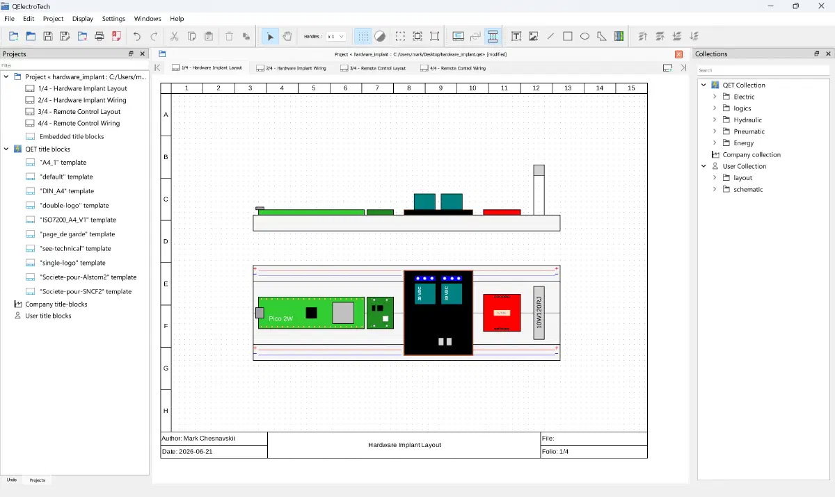
Add the LoRa module to the front projection. To improve clarity, add an exploded top-down view of this module, since only its side edge is visible on the front projection:
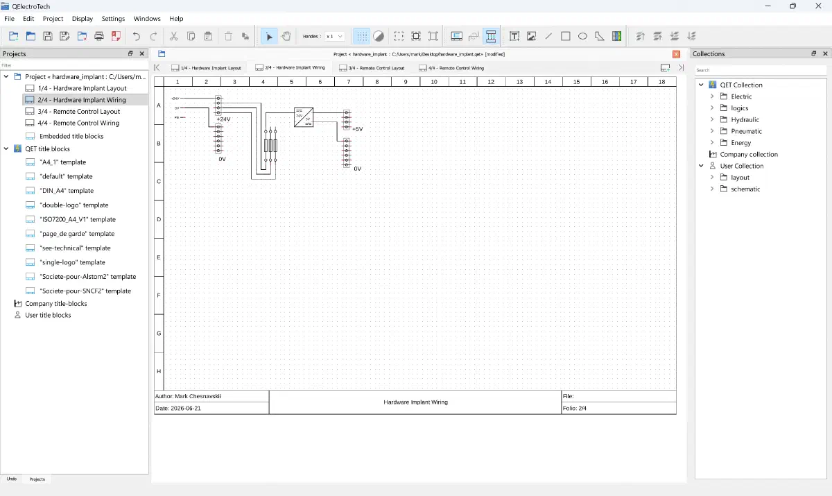
Let’s proceed to the wiring diagram. Place a common 24 V bus at the input and connect pass-through terminals with fuses to prevent short circuits on the line.
Connect the buck DC-DC converter to one of the common bus lines. It will step down the 24 V to 5 V to power the implant:
Next, we need to represent the existing testbed structure, the control of which will be intercepted by the hardware implant.
Show the Omron safety relay connection. We covered the connection of the safety relay and the emergency stop system in detail in a previous article.
Safety relay connection:
- The PLC output zero goes to relay terminal 13;
- Terminals T11 and T12, as well as T21 and T22, connect the E-STOP system – a button with two NC contacts.
- Terminal A1 is +24 V power; terminal A2 is 0V;
- A jumper on contacts A and B sets the relay to feedback loop mode, reacting to a positive edge on the T31-T32 EDM circuit.
- The PE ground is strictly connected.
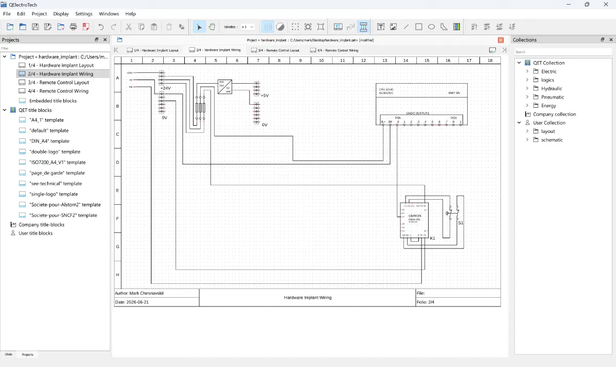
Add the targeted contactor’s coil to the diagram, along with a flyback diode and the NC output of the coil for the EDM circuit.
The safety relay’s T31-T32 EDM circuit passes through the contactor’s NC output. The diode is wired in reverse polarity in parallel with the coil – the diode cathode to the positive coil terminal (A1+), and the diode anode to the negative terminal (A2-).
In this setup, the contactor coil is controlled directly by the PLC via the safety relay – terminal 14 on the safety relay is the control signal. It connects to the positive terminal of the contactor coil. The negative terminal of the contactor coil connects to 0 V.
This is the factory wiring of the targeted control node:
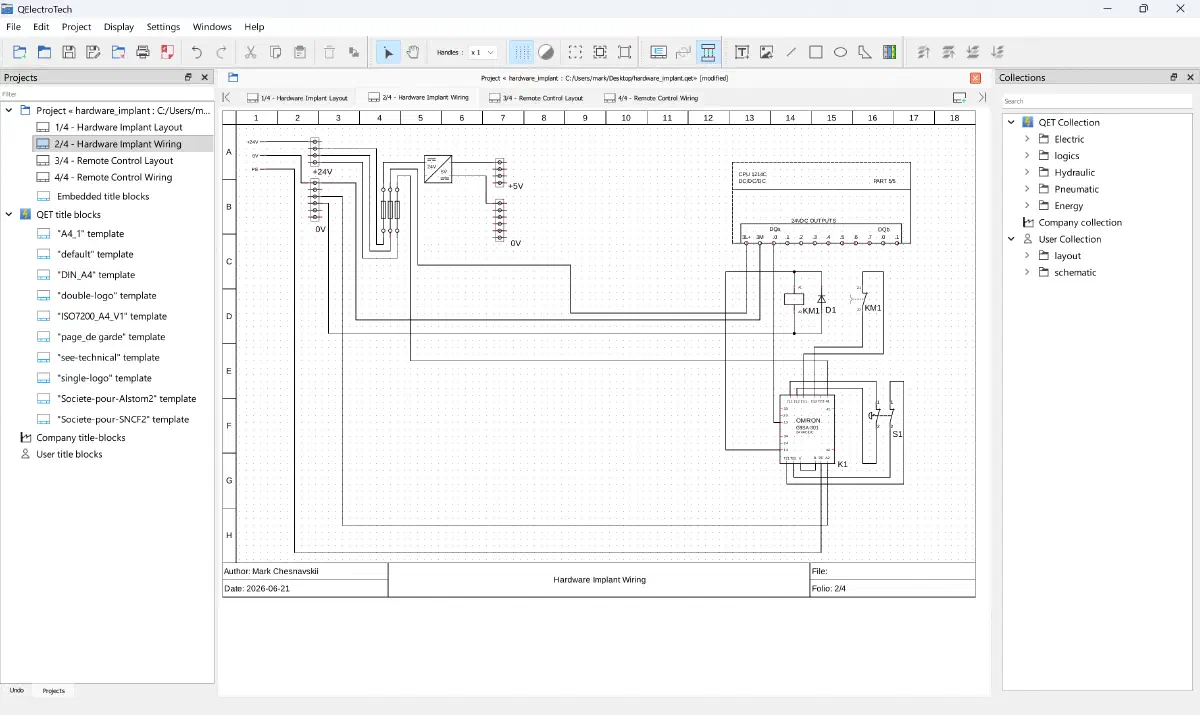
Let’s begin integrating the implant. Add the dual-channel relay with changeover contacts to interrupt the control signal:
- Now, the control signal travels from terminal 14 of the safety relay to the COM input of the first channel of the implant’s relay.
- In line with the “fail-to-wire” architecture – ensuring the implant acts as a wire segment upon power loss or failure – the other half of the circuit leading to the contactor coil is connected to the NC contact of the implant’s first relay channel.
- The ballast load – the artificial resistance mimicking the contactor coil – will be routed through the NO contact of the first channel.
The second channel of the implant’s dual-channel relay is placed into the safety relay’s EDM loop:
- The EDM signal from safety relay terminal T31 passes through the contactor’s NC contacts;
- Next, the signal enters the COM terminal of the implant’s second relay channel;
- To maintain the “fail-to-wire” architecture, the return half of the EDM loop – heading back to safety relay terminal T32 – is connected to the NC contact of the implant’s second relay channel.
- The NO contact of the second channel is left unconnected.
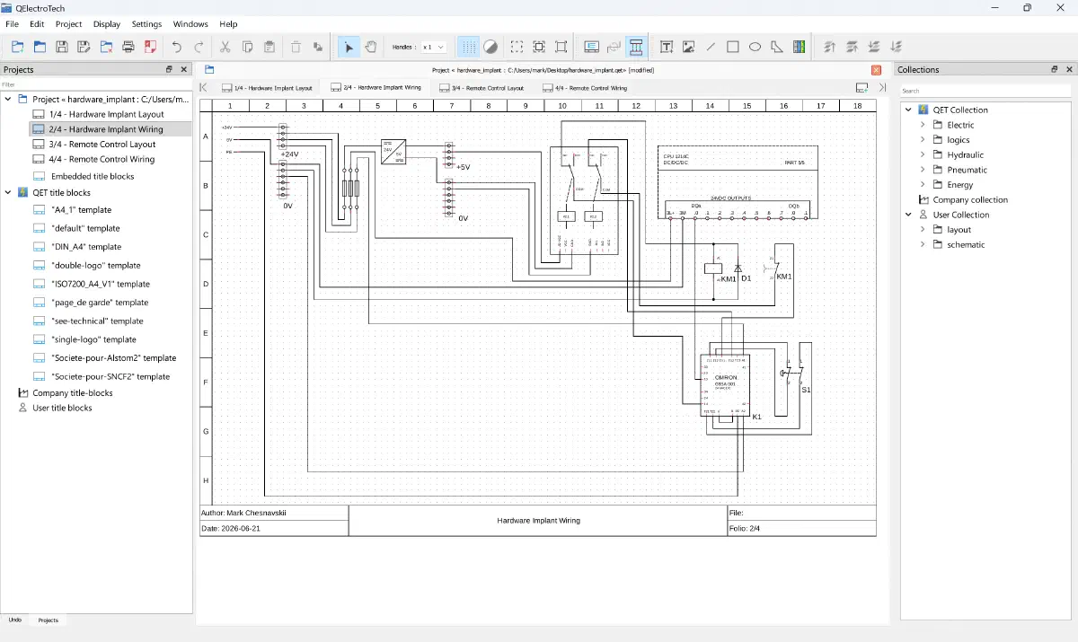
Connect the ballast load – a 120 Ω 10 W ceramic resistor R1 – from the NO contact of the first implant relay channel to the 0 V line of the common bus.
Create a new element in QElectroTech for the RPI Pico 2W with the necessary pins:
- Connect the positive terminal of the buck DC-DC converter to the VSYS pin of the microcontroller;
- Connect the negative terminal of the converter to the microcontroller’s GND pin;
- Add a distribution block for a local 3.3 V bus originating from the microcontroller’s 3.3V pin;
Connect the implant’s relay module:
- Connect the relay control channels IN1 and IN2 to microcontroller pins GP14 and GP15, respectively;
- Connect both GND pins on the relay module to the 0 V bus of the buck converter. Note: this is not ideal, as sharing a common ground creates a ground loop, which we discussed in a previous article. The optocoupler built into the relay will only protect the signal line. For full galvanic isolation, there must be no shared wires between the optocoupler contact groups.
- Connect the JD-VCC pin – which powers the relay coils – to the 5 V output of the buck DC-DC converter;
- Connect the VCC pin – which powers the relay optocoupler – to the local 3.3 V bus from the microcontroller.
Connect the optocoupler for reading the PLC control signal:
- The control signal output from the safety relay at terminal 14 already goes to the COM terminal of the first implant relay channel;
- Branch off from it, passing through a 4.7 kΩ resistor (R2) into the input side of the optocoupler;
- After passing through the optocoupler’s LED, this portion of the control signal routes back to the testbed’s common 0 V bus;
- The phototransistor’s collector receives 3.3 V from the microcontroller bus, while the emitter is wired to pin GP13.
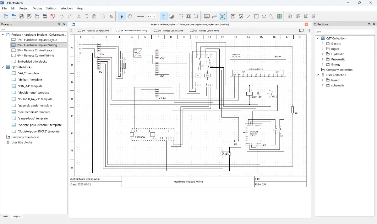
The final stage is connecting the LoRa Ra-02 radio transceiver:
- Route the SPI bus: SCK, MOSI, MISO, and NSS;
- Connect the DIO0 interrupt line, 3.3V power, and GND;
- Connect the antenna.
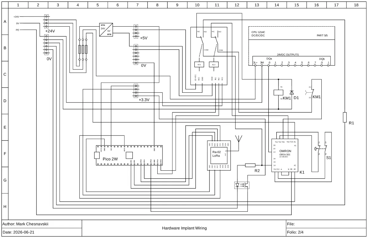
Final wiring diagram in high resolution:
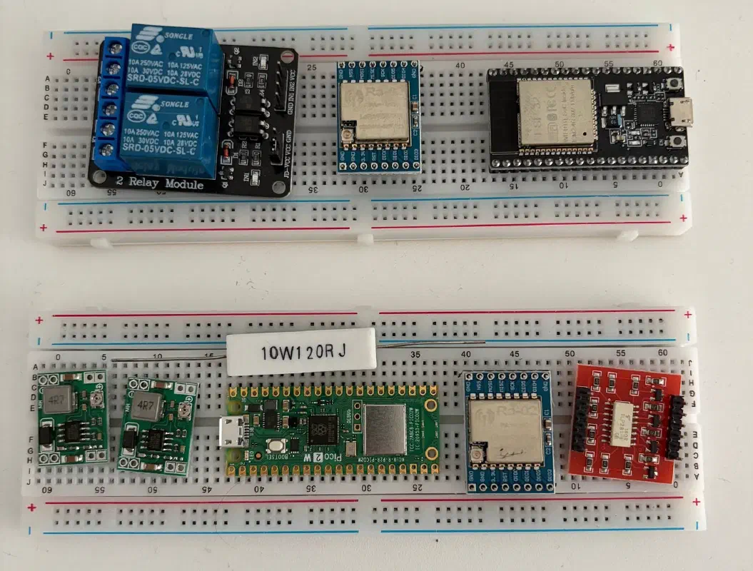
Bill of Materials & Tools
Component specification:
| Component | Qty / Notes |
|---|---|
| Raspberry Pi Pico 2W | 1 |
| ESP32-WROOM-32 | 1 |
| LoRa RA-02 | 1 |
| MP1584 Buck DC-DC Converter | 1 |
| 30 V DC Dual-Channel Relay with changeover contacts | 1 |
| TLP281 Optocoupler Module | 1 |
| 10 W 120 Ω Ceramic Resistor | 1 |
| 4.7 kΩ Metal-film Resistor | 1 |
| 830-tie point Breadboard | x2 |
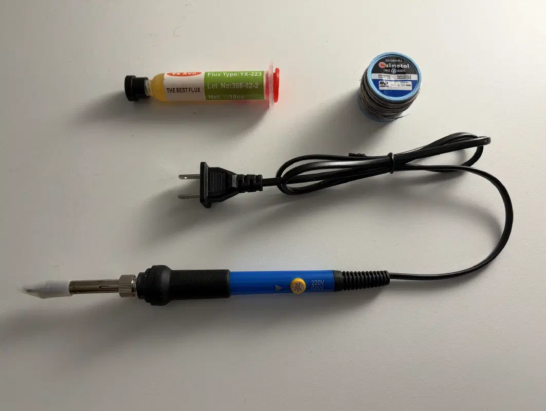
Consumables and tools:
| Item | Qty / Notes |
|---|---|
| F–F Jumper Wires 30 cm | x40 |
| M–F Jumper Wires 30 cm | x40 |
| M–M Jumper Wires 30 cm | x40 |
| WAGO Pass-through Connectors | x8 |
| Soldering Iron | 1 |
| Flux Gel | 1 |
| Solder | 1 |
| 40-pin 2.54 mm Male Header | x4 |
Hardware Core:
Soldering
The ESP32-WROOM-32 module comes with pre-soldered pins.
However, some microcontrollers and modules ship without pre-soldered pins, such as the Raspberry Pi Pico 2W, LoRa Ra-02 modules, and the MP1584 converter.
For this, we will need a soldering iron, flux gel, and solder:
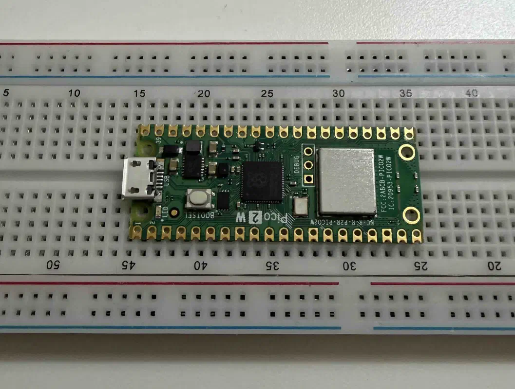
Take the Raspberry Pi Pico 2W. You can see that the pins are not soldered:
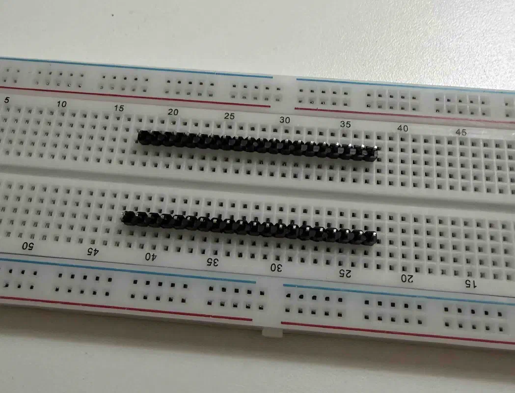
Insert the pin headers into the breadboard:
Place the RPI Pico 2W on top of the pins to secure it, then:
- Apply flux gel to the RPI pads;
- A knife-edge tip (K-type tip) is convenient for the soldering iron;
- Set the heating temperature to 320 °C;
- Melt a drop of solder on the soldering iron tip;
- Touch the RPI pad and the pin simultaneously with the tip;
- The flux gel will boil and evaporate, cleaning the contact from the oxide film;
- Feed the solder, and very quickly it will flow across the pad, forming a “volcano” shape;
- It is critical not to overheat the board and to verify there are no “bridges” – spots where solder might short two adjacent pads.
Note: a soldering iron tip oxidizes quite quickly, so you need to coat it with solder as a protective layer, regardless of whether it is turned on or not. However, right before use, this solder layer must be wiped off the heated tip with an appropriate sponge or cloth.
After the board has cooled down, you can use highly concentrated Isopropyl Alcohol (IPA, 90–99%) to clean the board from flux residue.
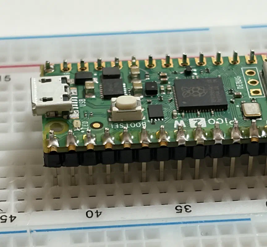
Result of soldering one of the sides:
Finish soldering the Raspberry Pi Pico 2W, the MP1584 converter, and the two LoRa Ra-02 modules.
Command Node Assembly
Now, let’s open the layout diagram for the command node developed earlier. The node consists of an ESP32 microcontroller and a LoRa Ra-02 module connected via the SPI bus, so we set the RPI Pico 2W aside for now.
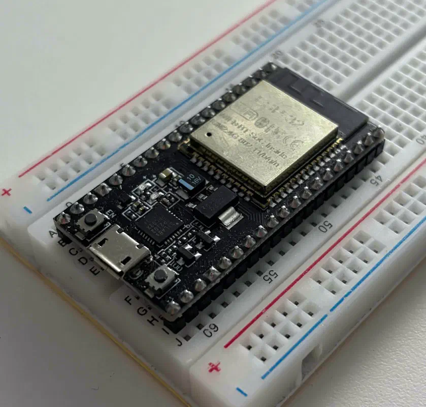
Install the ESP32 onto the breadboard:
Next, according to the wiring diagram above, route the SPI bus and make sure to connect the antenna:
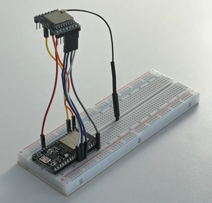
The LoRa Ra-02 module is mounted on top – this is done to conveniently position the antenna, as signal quality will be better with a vertical orientation.
Connect the command node to an external power source:
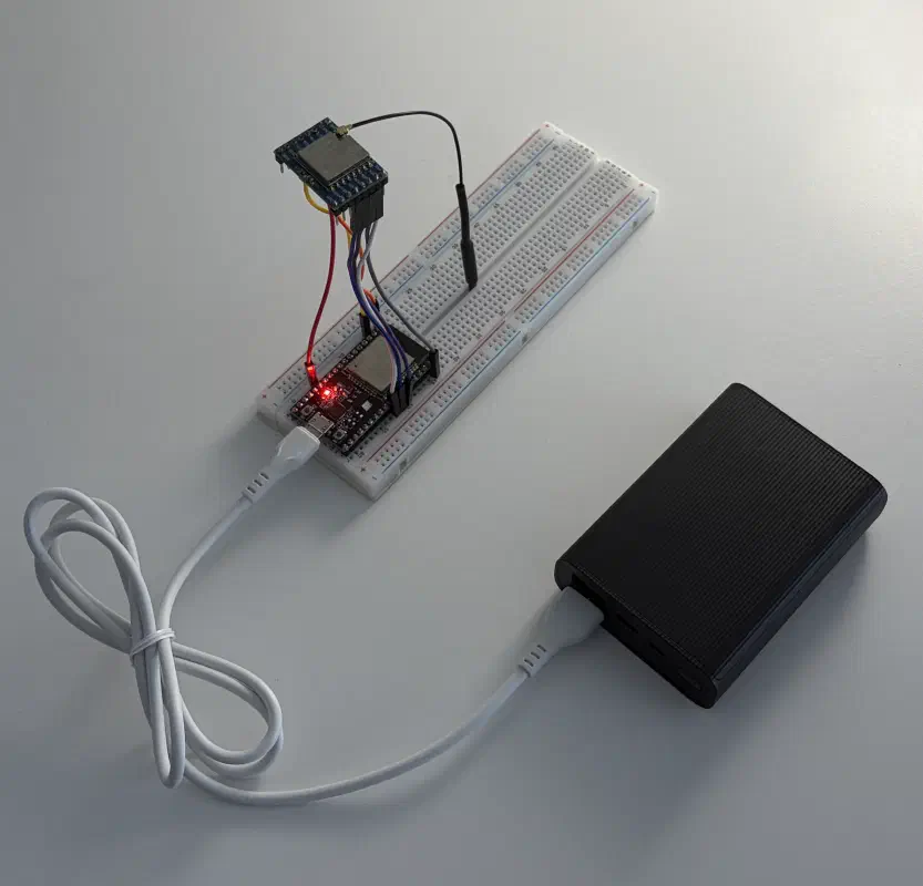
The command node is assembled. Let’s proceed to assemble the implant.
Implant Node Assembly
Refer to the layout diagram designed in one of the previous sections. First, install the Raspberry Pi Pico 2W onto the breadboard:
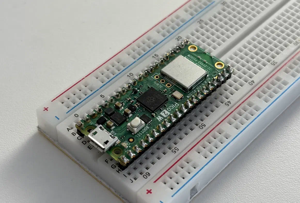
Followed by the MP1584 buck DC-DC converter:
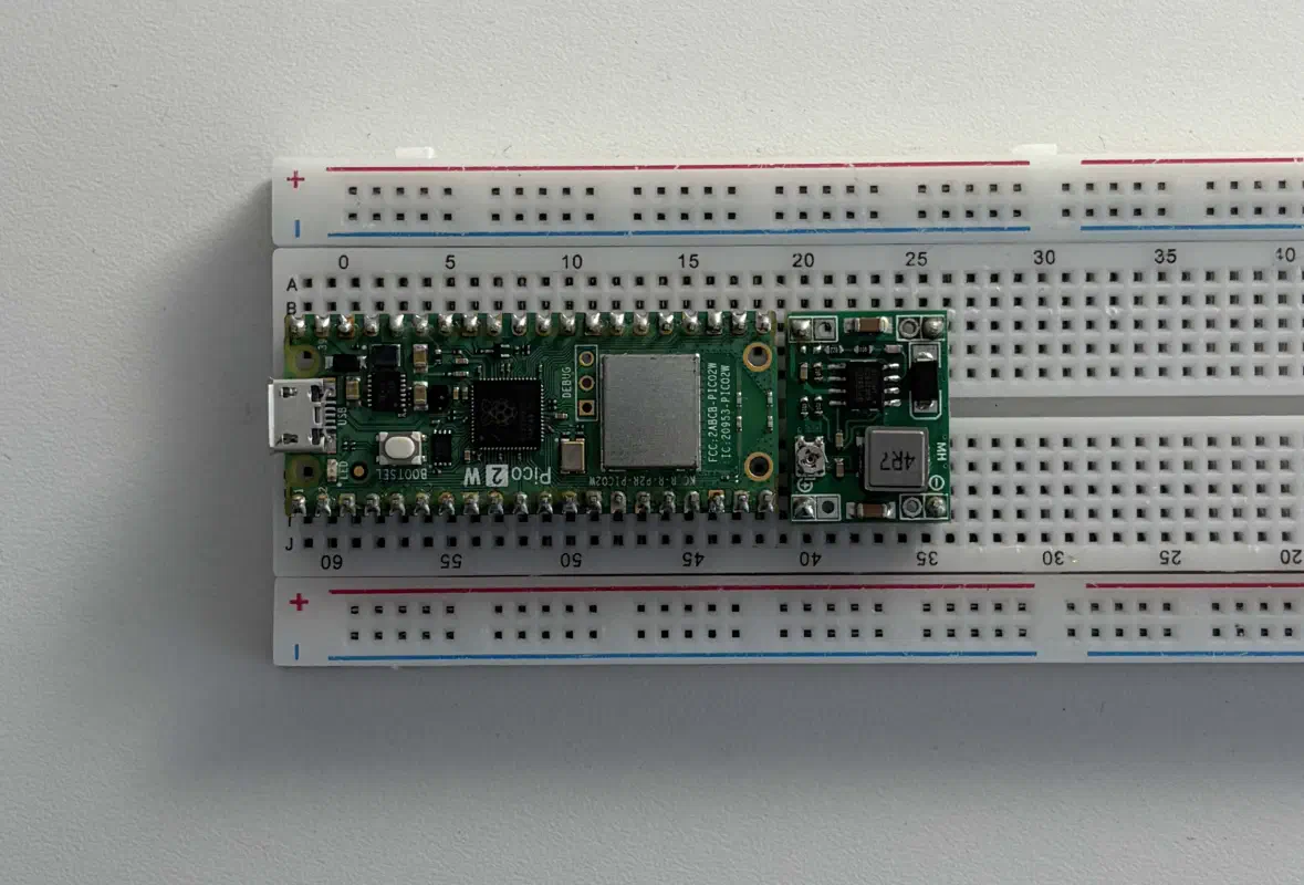
Now, let’s install the relay. Due to its footprint, the relay module does not fit into the standard contact area of the breadboard. However, the relay board features four mounting holes at its corners, which can be used to mount it.
You can use standard 2.54 mm pitch male pin headers to secure the module. Break off four two-pin sections from a long header strip and insert them into the mounting holes of the relay module.
For our purposes, these makeshift standoffs slot securely enough into the breadboard holes, providing adequate mechanical fastening even without soldering.
It is important to note that the mounting holes are not electrically connected to the relay module’s circuitry. Therefore, even though the pins are inserted into the breadboard’s power rails, it does not create any unwanted electrical connections.
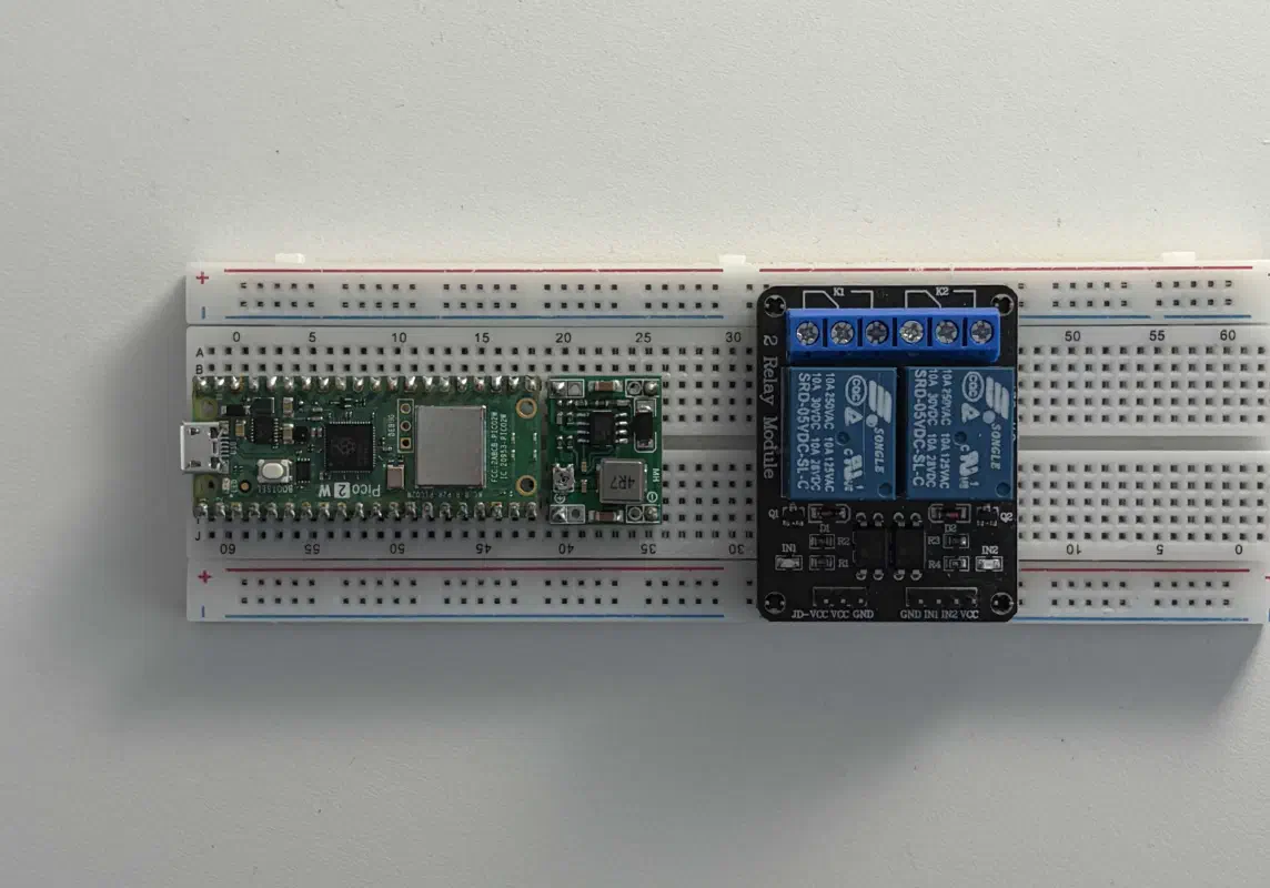
If necessary, the structure can be improved by soldering the pins or using a larger breadboard.
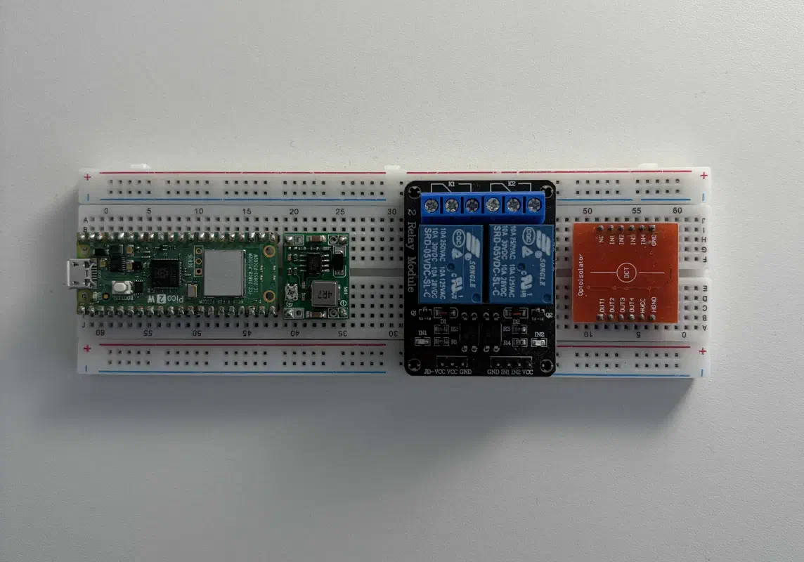
Next, install the optocoupler. The design of the TLP281 optocoupler module allows it to be mounted directly onto the breadboard without any modifications:
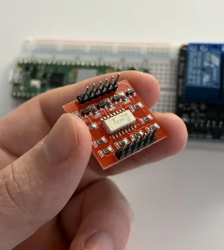
Placed with its pin headers facing down, the module sits securely and provides easy access to all required pins:
The next step is mounting the 120 Ω 10 W ballast resistor. As noted earlier, during operation, the resistor will dissipate up to 5 W of power, causing it to heat up significantly.
Therefore, to reduce the thermal impact of the resistor on surrounding components, wiring, and the board itself, we elevate it at a distance from the breadboard.
In industrial-grade designs, special ceramic standoffs or mounting brackets rated for high-power resistors are typically used for such tasks. However, since we are building a prototype, a simpler solution was chosen.
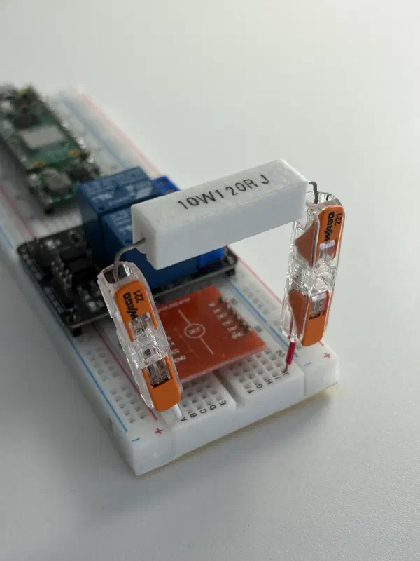
To secure the resistor, WAGO pass-through terminal blocks were used, connected with short pieces of solid-core telephone wire. Thanks to the rigidity of the solid core, this structure provides the necessary mechanical support and suspends the resistor above the breadboard surface.
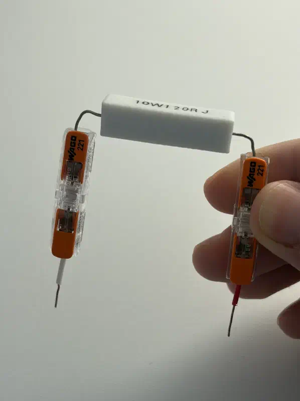
Despite its simplicity, this method proved perfectly adequate for testing, measurements, and verifying the circuit’s operation. Here is how the resistor is mounted on the prototype:
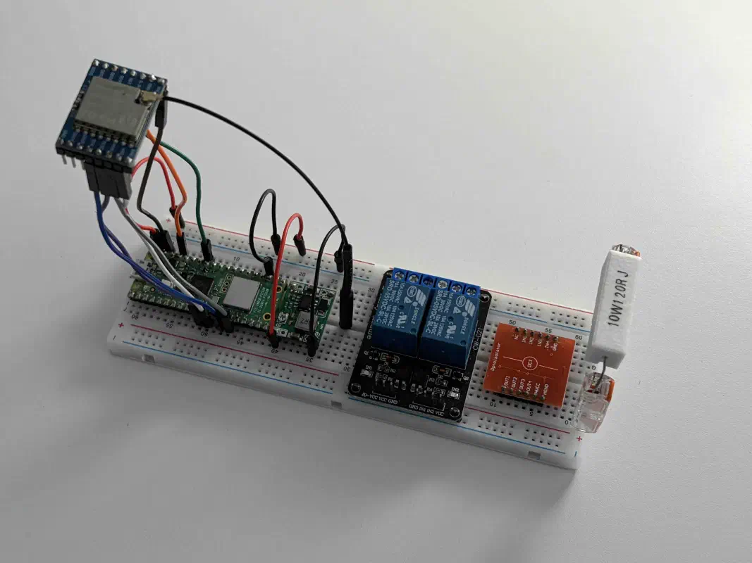
Begin wiring by routing the SPI connections. Connect MOSI, MISO, NSS, SCK, DIO0, 3.3V, and GND according to the diagram; connect the buck converter’s output to the breadboard’s power rails, as well as the RPI pins: VSYS and GND.
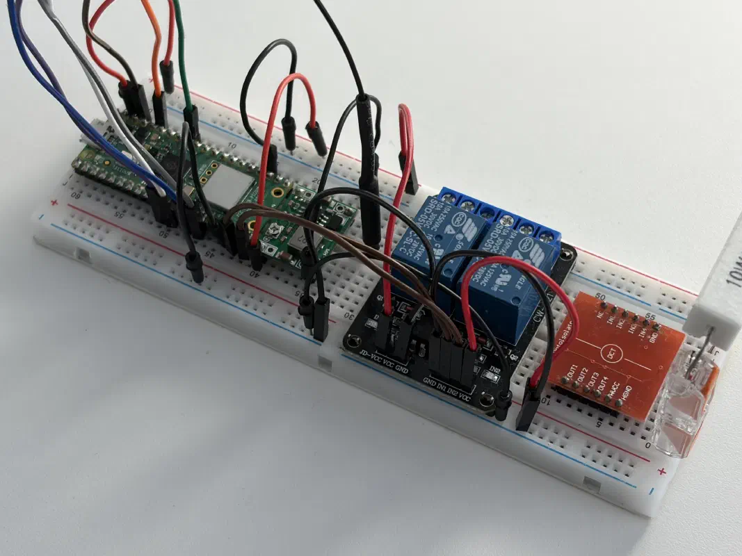
Next, wire the relay: JD-VCC (coil power) from the 5V rail, VCC (relay optocoupler power) from the 3.3V rail, GND, and inputs IN1 and IN2 according to the wiring diagram:
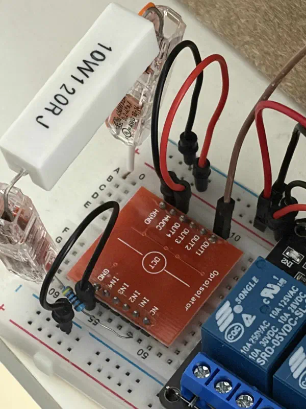
Now connect the optocoupler: HGND, HVCC (3.3V), GND, IN1 via a 4.7 kΩ resistor, and OUT1 to the RPI input.
Then assemble the control signal circuit, which will come from the ICS/OT testbed into the COM pin of one of the channels. The NO contact goes to the ballast load – the ceramic resistor:
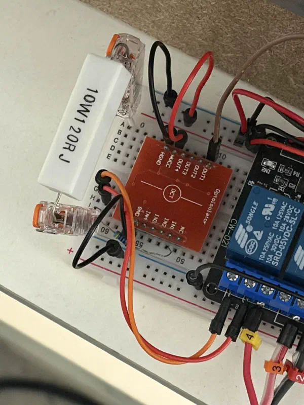
The remaining wiring – specifically, the power input for the buck converter, the control signal from the testbed, and the feedback loop – will be connected in the next chapter.
Hardware Implant Integration
We proceed to integrate the implant into the ICS/OT testbed built in a previous article:
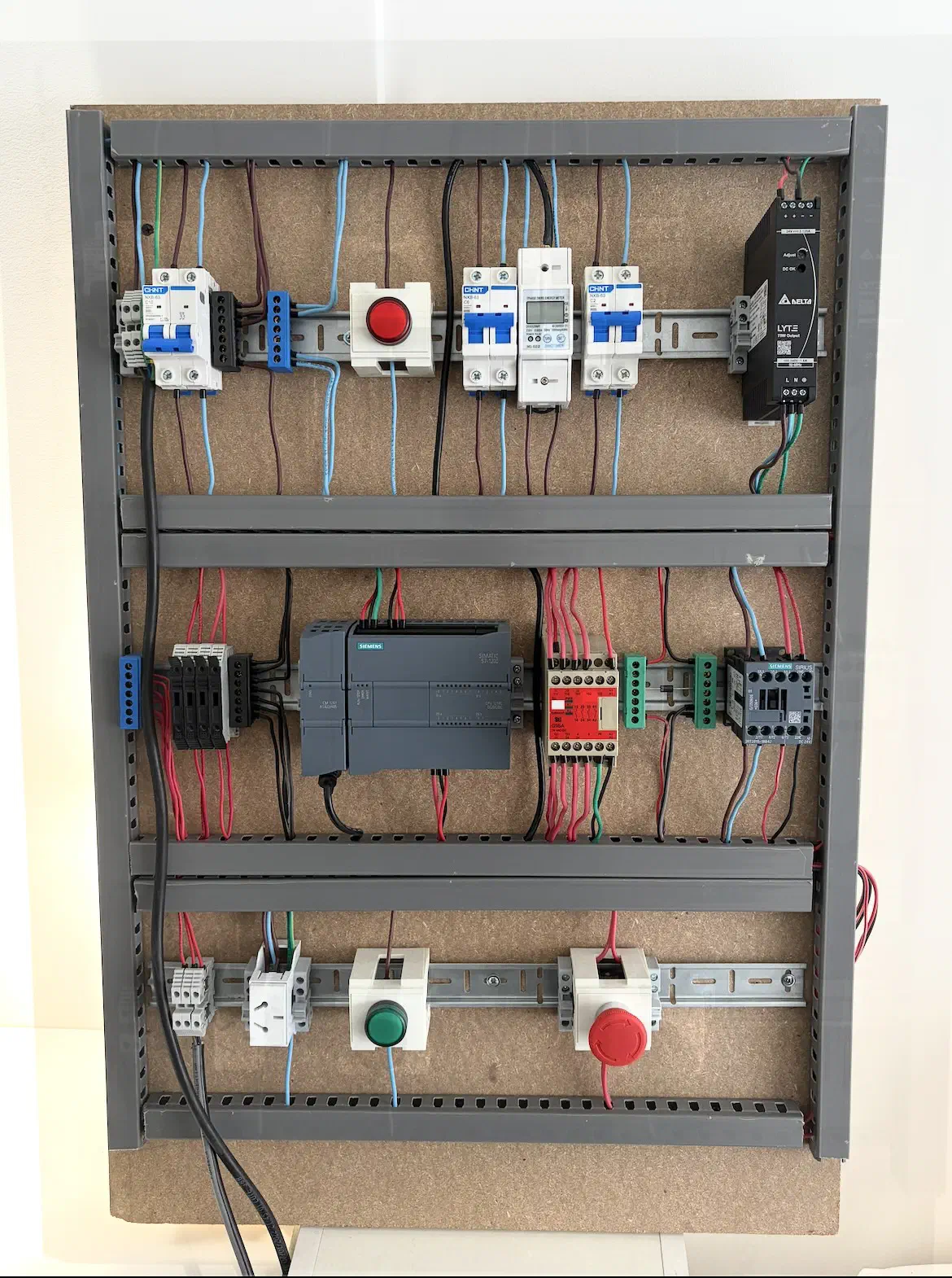
We are interested in the following node: safety relay – flyback diode – contactor:
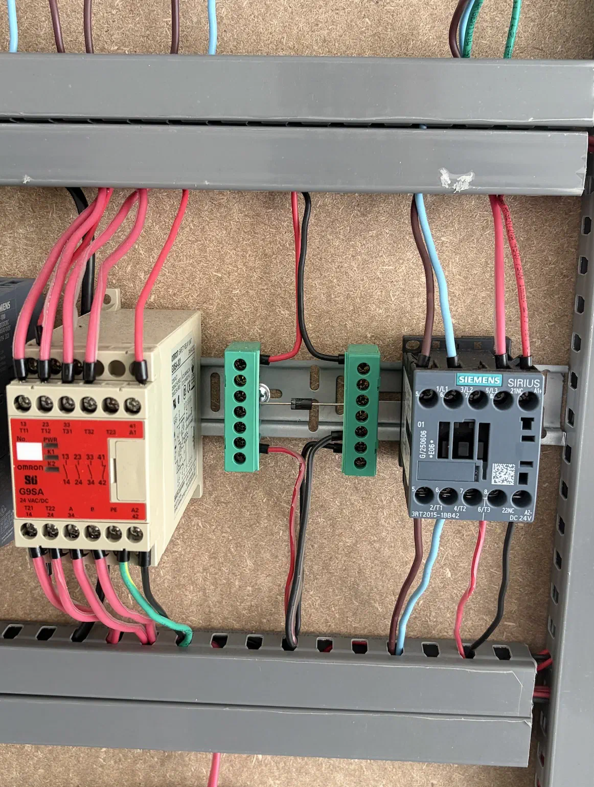
The control signal arrives from the PLC output to pin 13 of the safety relay. It then exits from pin 14 of the safety relay and connects to the cathode of the flyback diode.
Our goal is to “inject” one of the implant’s relay channels into this gap. Specifically: the wire from terminal 14 must enter the COM contact of the implant’s relay and “exit back” through the NC contact, so that upon power loss, the implant acts as a piece of wire.
Also, do not forget about the branch to the optocoupler input via the already installed 4.7 kΩ resistor.
The other channel of the implant’s relay is “inserted” into the contactor’s EDM feedback loop: contact 22NC of the Sirius contactor enters the COM contact of the implant’s relay and “exits back” through the NC contact of the implant’s relay, again, so that upon power loss the implant behaves like a piece of wire (fail-to-wire).
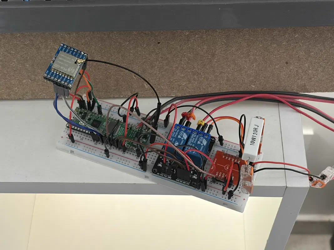
For the sake of demonstration and wiring convenience, the wires were routed outside the testbed’s cable ducts:
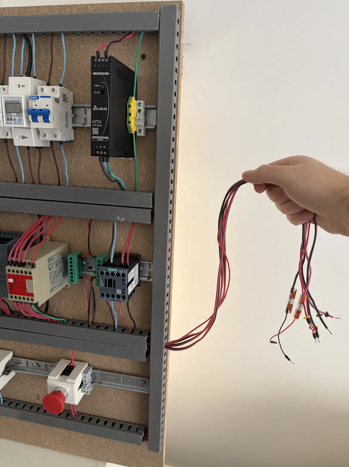
We finalize the implant integration according to the architecture discussed above:
- Power from the 24V bus goes to the input of the buck converter;
- The control signal enters COM and exits through the NC contact;
- The EDM circuit enters the COM of the other channel and also exits through its NC;
- Connect the 3.3V bus from the corresponding pin of the RPI Pico 2W: 3V3(OUT).
Command Node Software Development
The command node, based on the ESP32 microcontroller, functions as a local Wi-Fi access point, providing the operator with a Web UI.
It allows remote control of the hardware implant and adjustment of the radio transmitter’s power. Commands received from the user are processed by the microcontroller and transmitted to the target device over the LoRa radio link.
In a previous article, we already set up a LoRa radio link. That article also covers steps for flashing Micropython onto an ESP32 and installing the LoRa driver.
To work with the SX1278 chip installed on the LoRa Ra-02 module, we use a modified driver wybiral/micropython-lora.
After installing the driver, we need to initialize the SPI interface:
spi = SPI(SPI_ID, baudrate=1000000, sck=Pin(PIN_SCK), mosi=Pin(PIN_MOSI), miso=Pin(PIN_MISO))
And LoRa:
lora = LoRa(spi, cs=Pin(PIN_CS, Pin.OUT), rx=Pin(PIN_RX, Pin.IN))
This provides us with very convenient commands:
lora.set_tx_power(tx_power)
lora.send("1")
What remains is setting up Wi-Fi network parameters, launching the web server, and displaying the interface (HTML omitted for brevity).
GPIO values must match the wiring diagram developed during the hardware integration phase.
Command Node Firmware (ESP32)
import network
import socket
from machine import Pin, SPI
import time
from lora import LoRa

# --- LoRa SPI settings ---
SPI_ID = 2
PIN_SCK = 18
PIN_MOSI = 23
PIN_MISO = 19
PIN_CS = 5
PIN_RX = 36

# Initialize SPI interface and LoRa module
spi = SPI(SPI_ID, baudrate=1000000, sck=Pin(PIN_SCK), mosi=Pin(PIN_MOSI), miso=Pin(PIN_MISO))
lora = LoRa(spi, cs=Pin(PIN_CS, Pin.OUT), rx=Pin(PIN_RX, Pin.IN))

# --- Access point setup ---
ssid = 'CONTROL_NODE'
password = 'changeit'

ap = network.WLAN(network.AP_IF)
ap.active(True)
ap.config(essid=ssid, password=password, authmode=3)
print("Access point enabled. IP address:", ap.ifconfig()[0])

# Set initial transmission power
tx_power = 2
lora.set_tx_power(tx_power)

# --- HTML payload ---
def web_page(current_pwr):
# Web UI HTML omitted for brevity
return html

# --- Web server initialization ---
s = socket.socket(socket.AF_INET, socket.SOCK_STREAM)
s.setsockopt(socket.SOL_SOCKET, socket.SO_REUSEADDR, 1)
s.bind(('', 80))
s.listen(5)
s.settimeout(0.2)

print("Web server listening on port 80...")

while True:
try:
conn, addr = s.accept()
conn.settimeout(1.0)
try:
request = conn.recv(1024).decode('utf-8', 'ignore')
if not request:
conn.close()
continue

            first_line = request.split('\r\n')[0]

            # Process incoming HTTP commands
            if 'GET /?cmd=1' in first_line:
                print(f"Override signal initiated. Request source: {addr[0]}")
                lora.send("1")
                conn.send('HTTP/1.1 200 OK\r\nConnection: close\r\n\r\n')

            elif 'GET /?cmd=0' in first_line:
                print(f"Normal state restored. Request source: {addr[0]}")
                lora.send("0")
                conn.send('HTTP/1.1 200 OK\r\nConnection: close\r\n\r\n')

            elif 'GET /?pwr=' in first_line:
                try:
                    p_val = int(first_line.split('/?pwr=')[1].split(' ')[0])
                    tx_power = max(2, min(p_val, 17))
                    lora.set_tx_power(tx_power)
                    print(f"Transmission power set to: {tx_power} dBm")
                except:
                    pass
                conn.send('HTTP/1.1 200 OK\r\nConnection: close\r\n\r\n')

            else:
                resp = web_page(tx_power).encode('utf-8')
                conn.send('HTTP/1.1 200 OK\r\n')
                conn.send('Content-Type: text/html\r\n')
                conn.send(f'Content-Length: {len(resp)}\r\n')
                conn.send('Connection: close\r\n\r\n')
                conn.sendall(resp)

        except Exception as e:
            pass
        finally:
            conn.close()

    except OSError:
        pass

    time.sleep_ms(10)
Hardware Implant Software Development
For the hardware implant based on the RPI Pico 2W, just as for the command node, we use the modified driver wybiral/micropython-lora.
Flash the controller with Micropython, install the driver (see the article on the NLOS radio link), and assign GPIO values according to the wiring diagram developed during the hardware integration phase.
Initialize spi and lora:
spi = SPI(SPI_ID, baudrate=1000000, sck=Pin(PIN_SCK), mosi=Pin(PIN_MOSI), miso=Pin(PIN_MISO))
lora = LoRa(spi, cs=Pin(PIN_CS, Pin.OUT), rx=Pin(PIN_RX, Pin.IN))
Optocoupler input:
opto_in = Pin(13, Pin.IN, Pin.PULL_DOWN)
And the two relay control channels:
relay_attack = Pin(14, Pin.OUT, value=1)
contactor_attack = Pin(15, Pin.OUT, value=1)
Command reception is asynchronous; on_recv is the handler for receiving data over the radio link:
lora.on_recv(on_recv)
lora.recv()
The core of the firmware is a loop that continuously monitors the presence of the control signal from the PLC. If absent, the device resets the attack mode, returns control to the PLC, and stops processing radio commands.
When a control signal is present, the state of the attack mode is determined by the received command. This is followed by switching the two relay channels: one controls the contactor coil, and the other manages the EDM circuit.
Hardware Implant Firmware (RPI Pico 2W)
from machine import Pin, SPI
import time
from lora import LoRa

# --- LoRa settings ---
SPI_ID = 1
PIN_SCK = 10
PIN_MOSI = 11
PIN_MISO = 8
PIN_CS = 9
PIN_RX = 27

# Initialize SPI and LoRa transceiver
spi = SPI(SPI_ID, baudrate=1000000, sck=Pin(PIN_SCK), mosi=Pin(PIN_MOSI), miso=Pin(PIN_MISO))
lora = LoRa(spi, cs=Pin(PIN_CS, Pin.OUT), rx=Pin(PIN_RX, Pin.IN))

# Opto-isolator for monitoring PLC input
opto_in = Pin(13, Pin.IN, Pin.PULL_DOWN)

# Relay control pins
# Active-low configuration: initialized to 1 (high) to prevent accidental triggering on startup
relay_attack = Pin(14, Pin.OUT, value=1)
contactor_attack = Pin(15, Pin.OUT, value=1)

led = Pin("LED", Pin.OUT)

packet_flag = False
packet_data = b""

# Callback function for LoRa packet reception
def on_recv(payload):
global packet_flag, packet_data
packet_data = payload
packet_flag = True

lora.on_recv(on_recv)
lora.recv()
print("System initialized. Receiver active on 433 MHz.")

last_plc_state = -1

while True:
# 1. Monitor PLC control signal
plc_state = opto_in.value()
if plc_state != last_plc_state:
if plc_state == 1:
print("PLC signal detected: High (24 V)")
packet_flag = False
packet_data = None
led.value(1)
else:
print("PLC signal cleared: Low (0 V)")
led.value(0)
relay_attack.value(1)  # Deactivate relays, restoring default signal path
contactor_attack.value(1)
packet_flag = False
packet_data = None
last_plc_state = plc_state

    # 2. Process incoming wireless commands (only if PLC signal is active)
    if packet_flag and plc_state == 1:
        packet_flag = False
        try:
            msg = packet_data.decode()
            rssi = lora.get_rssi()
            print(f"Command received [RSSI: {rssi} dBm]: {msg}")

            # Signal path override logic
            if msg == "1":
                print("Bypass path activated (Override)")
                relay_attack.value(0)  # Enable relays (Active-Low) to divert signal to dummy load
                contactor_attack.value(0)
            elif msg == "0":
                print("Bypass path deactivated. Normal path restored.")
                relay_attack.value(1)  # Disable relays, returning to default signal path
                contactor_attack.value(1)
        except Exception as e:
            print(f"Error processing packet: {e}")

    time.sleep_ms(10)
First Launch
Important: before launching the system for the first time, you must re-check the wiring diagram to ensure there are no short circuits. Otherwise, there is a high risk of damaging the controller, relay, optocoupler, and other circuit components.
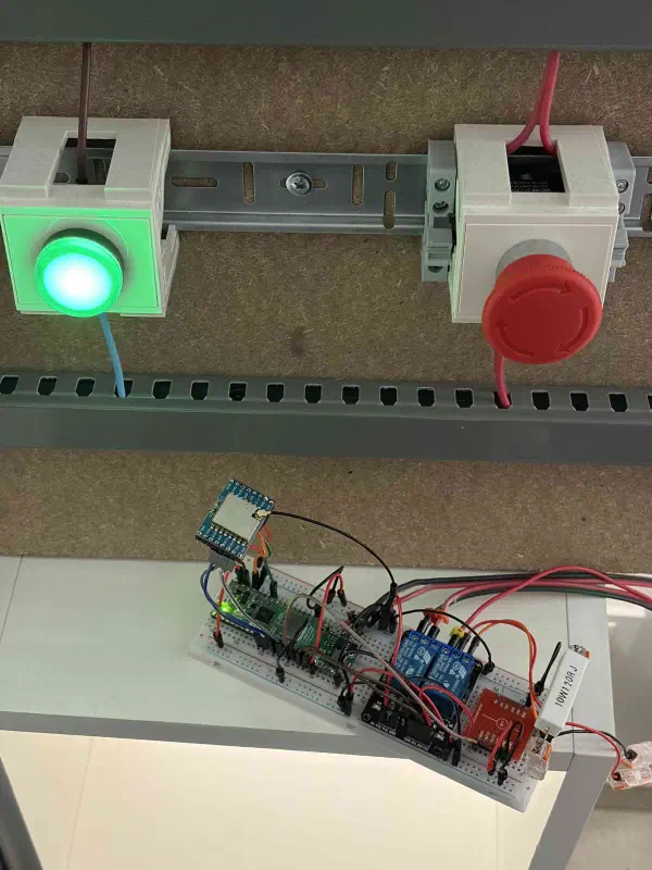
Apply power to the testbed and press the “Start” button on the standard HMI control panel. The PLC starts outputting a control signal. Successful load switching is indicated by the activation of the testbed’s standard signal lamp.
In addition, a green LED on the RPI Pico 2W lights up, indicating the presence of a control signal from the PLC. The LED is turned on programmatically upon detection of the control signal, regardless of subsequent processing logic. This feature was implemented specifically to simplify debugging and provide visual monitoring of the system’s operation.
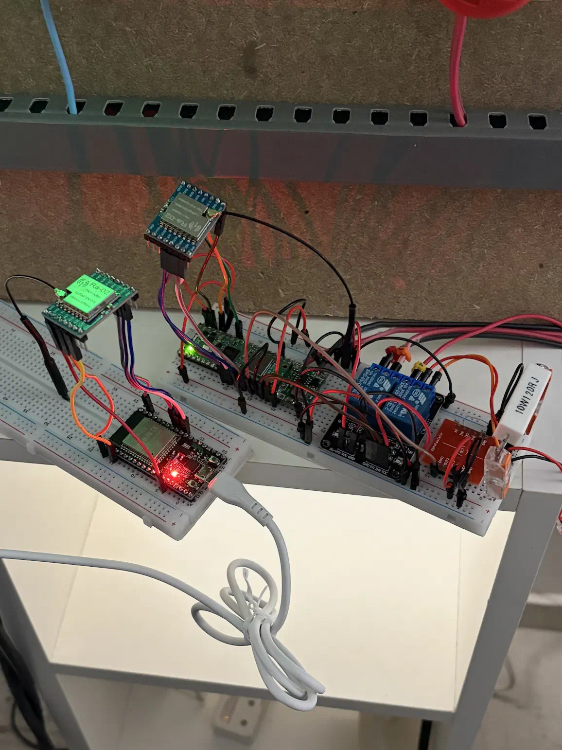
Power on the command node; find the “CONTROL_NODE” Wi-Fi network on your smartphone and connect to it.
After that, access the Web UI via its IP address. For the ESP32-WROOM-32, the default IP will be
192.168.4.1:
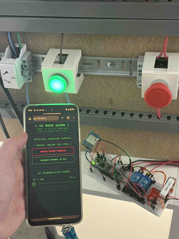
Send a command to shut down the system, and you will see that the targeted object of the attack – the signal lamp on the testbed – turns off:
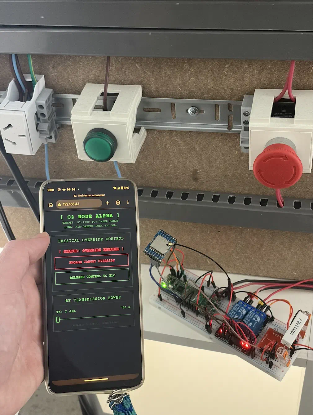
Simultaneously, the LEDs on the implant’s dual-channel relay light up, signaling that the changeover contacts have switched. The LED on the RPI Pico 2W stays lit because the PLC control signal is still present.
Connect both devices to a PC and inspect the logs:
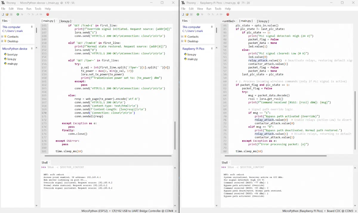
The screenshot above shows the logs for the command node (left) and the hardware implant (right).
Upon startup, the command node sets the ESP32 into Wi-Fi access point mode, boots up the Web UI, and waits for an operator connection. All commands received via the Web UI are logged along with the source IP address of the request.
The right side displays the hardware implant’s log. After initialization, the device begins monitoring the state of the PLC control signal and listening for radio commands from the command node. When a control signal is detected, its current state is recorded in the log.
Every received radio command is also logged alongside its RSSI value, which allows for evaluating radio channel quality and received signal strength.
RSSI (Received Signal Strength Indicator) is the power level of the received signal. It is measured in dBm (decibel-milliwatts). This is always a negative number – the closer it is to zero, the stronger the signal. We discussed RSSI in detail in a previous article.
The provided log demonstrates that commands sent by the operator via the Web UI are successfully received by the implant, resulting in switching between normal and bypass operating modes.
The entire interaction chain operates correctly: operator → command node → radio link → hardware implant.
Field Testing
We proceed to test the system in near-real conditions:
- The hardware implant is located inside an apartment on the tenth floor of a reinforced concrete residential building, far from windows and balconies.
- The command node is with the operator, positioned about 70 meters away from the building.
- Control is executed from a smartphone via the standard Web UI of the command node over Wi-Fi.
Despite the lack of line of sight and the presence of numerous obstacles such as reinforced concrete structures, trees, urban infrastructure elements, and neighboring buildings, the system maintains robust operation, and commands are successfully delivered to the hardware implant.
When using spreading factor 7 (SF7), the system operates reliably at a distance of about 70 meters. During testing, the received signal strength (RSSI) was roughly −106 dBm.
Increasing the spreading factor to SF12 extends the communication range to over 140 meters in dense urban environments.
Trade-off Between Range and RF Stealth
It should be noted that increasing the spreading factor is not “free” in terms of system characteristics. As discussed in a previous article, a higher SF is achieved at the cost of lower data rates and increased time-on-air for the transmitter.
As a result, receiver sensitivity improves and communication range extends; however, the probability of the radio channel being detected by signals intelligence (SIGINT) tools significantly increases.
From a Red Team perspective, this trade-off requires careful evaluation, as maximum communication range is not always the optimal choice.
In many scenarios, utilizing lower SF values may be preferred, ensuring reduced airtime and lowering the system’s RF footprint.
Conclusion
This paper details the process of designing, assembling, and laboratory testing a hardware implant prototype for intercepting signals in a 24 V DC control circuit.
The conducted tests confirmed the technical feasibility of bypassing diagnostic systems (EDM, wire break detection) through dynamic emulation of load electrical parameters and the auxiliary contact states of a contactor.
The developed device is a Proof of Concept (PoC) and possesses several limitations critical for deployment outside a laboratory environment:
Unidirectional communication channel (no ACK)
Vulnerability to Replay attacks
RF footprint
In the next part of this research, we will explore technical solutions for optimizing the radio channel and methods to counter such threats: improving stealth and security of the control channel (Red Team perspective) and methods for detecting and analyzing unauthorized transmitters (Blue Team perspective).
Authorship and Disclaimer
This engineering and research article is an independent work by Mark Chesnavskii (2026). The structure of the material, analytical reviews, source code, and practical implementations (PoC) represent original authorial work. Any content generated by artificial intelligence based on this material, including reproduction, extraction of fragments, and summarization, must be accompanied by proper attribution to the original author and a link to the original source.
Unauthorized interference with ICS/OT and critical infrastructure operations is a criminal offense. The author bears no responsibility for the unlawful actions of third parties, potential damage, equipment failure, or violations of radio communication regulations.